- ASIC
- バッテリー マネージメントIC
- クロックとタイミングソリューション
- ESDおよびサージ保護デバイス
- 自動車用イーサネット
- 評価ボード
- 高信頼性(HiRel)
- アイソレーター
- メモリ
- マイクロコントローラー
- パワー
- RF
- セキュリティ ソリューションおよびスマートカードソリューション
- センサー技術
- 小信号トランジスタおよびダイオード
- トランシーバー
- ユニバーサル シリアル バス(USB)
- ワイヤレス接続
- Search Tools
- Technology
- Packages
- Product Information
- ご注文
- 概要
- 組込みフラッシュIPソリューション
- フラッシュプラスRAM MCPソリューション
- F-RAM (強誘電体RAM)
- NORフラッシュ
- nvSRAM (不揮発性 SRAM)
- PSRAM – 擬似スタティックRAM
- 耐放射線・高信頼性メモリ
- SRAM (スタティック RAM)
- ウェーハおよびダイメモリソリューション
- 概要
- AURIX™ TriCore™ MCU
- PSOC™ MCU
- TRAVEO™ T2G MCU
- XMC™ MCUs
- レガシーMCU
- MOTIX™ モーター制御SoC/SiP
- 概要
- アンテナクロススイッチ
- アンテナチューナー
- バイアスと制御
- カプラ
- ドライバアンプ
- 耐放射線マイクロ波とRF
- ローノイズアンプ (LNA)
- 高周波ダイオード
- RFスイッチ
- RFトランジスタ
- ワイヤレス制御向けレシーバー
- 概要
- Calypso®製品
- CIPURSE™ 製品
- 非接触メモリ
- OPTIGA™の組込みセキュリティ ソリューションの詳細
- SECORA™セキュリティソリューション
- セキュリ ティコントローラー
- スマートカードモジュール
- 政府ID向けスマートソリューション
- 概要
- ToF 3D イメージセンサー
- 電流センサー
- ガスセンサー
- 誘導型位置センサー
- MEMSマイクロフォン
- 圧力センサー
- レーダーセンサー
- 磁気位置センサー
- 磁気速度センサー
- Capacitive sensors
- Temperature sensors
- Battery sensors
- Digital X-ray
- Computed tomography
- Sensor interface ASICs
- 概要
- USB 2.0 ペリフェラル コントローラー
- USB 3.2 ペリフェラル コントローラー
- USB ハブ コントローラー
- USB PD高電圧マイクロコントローラー
- USB-C AC-DC および DC-DC 充電ソリューション
- USB-C充電ポートコントローラー
- USB-Cパワーデリバリー コントローラー
- 概要
- AIROC™ オートモーティブワイヤレス
- AIROC™ Bluetooth®およびマルチプロトコル
- AIROC™ コネクトテッドMCU
- AIROC™ Wi-Fi + Bluetooth®コンボ
- AIROC™ Ultra-Wide Band Solutions
- 概要
-
32 ビット TriCore™ AURIX™ – TC2x
- 概要
- AURIX™ ファミリー – TC21xL
- AURIX™ファミリー – TC21xSC (ワイヤレス充電)
- AURIX™ ファミリー – TC22xL
- AURIX™ ファミリー – TC23xL
- AURIX™ ファミリー – TC23xLA (ADAS)
- AURIX™ ファミリー – TC23xLX
- AURIX™ ファミリー – TC264DA (ADAS)
- AURIX™ ファミリー – TC26xD
- AURIX™ ファミリー – TC27xT
- AURIX™ ファミリー – TC297TA (ADAS)
- AURIX™ ファミリー – TC29xT
- AURIX™ファミリー – TC29xTT (ADAS)
- AURIX™ ファミリー – TC29xTX
- AURIX™ TC2xx (エミュレーションデバイス)
-
32 ビット TriCore™ AURIX™ – TC3x
- 概要
- AURIX™ ファミリー TC32xLP
- AURIX™ ファミリー – TC33xDA
- AURIX™ ファミリー - TC33xLP
- AURIX™ ファミリー – TC35xTA (ADAS)
- AURIX™ ファミリー – TC36xDP
- AURIX™ ファミリー – TC37xTP
- AURIX™ ファミリー – TC37xTX
- AURIX™ ファミリー – TC38xQP
- AURIX™ ファミリー – TC39xXA (ADAS)
- TC39xXX/XP
- AURIX™ ファミリー – TC3Ex
- AURIX™ TC37xTE (エミュレーションデバイス)
- AURIX™ TC39xXE (エミュレーションデバイス)
- 32 ビット TriCore™ AURIX™ - TC4x
- 概要
- PSOC™ 4 Arm® Cortex® -M0/M0+
- PSOC™ 4 HV Arm® Cortex® -M0+
- PSOC™ 5 LP Arm® Cortex® -M3
- PSOC™ 6 Arm® Cortex®-M4 / M0+
- PSOC™マルチタッチタッチスクリーンコントローラー
- PSOC™ Control C3 Arm® Cortex®-M33
- 自動車用PSOC™ 4 Arm® Cortex®-M0/M0+
- PSOC™ Edge Arm® Cortex® M55/M33
- PSOC™ Control C1 Arm® Cortex®-M0
- 概要
- ボディ用32ビットTRAVEO™T2G Arm® Cortex®
- クラスター用の 32 ビット TRAVEO™ T2G Arm® Cortex®
- 概要
- 32ビットMCU
- レガシー8ビット/16ビットマイクロコントローラー
- その他レガシーマイクロコントローラー
- 32ビットFM Arm® Cortex® マイクロコントローラー
- センシングコントローラー
- 概要
- 整流ブリッジおよびACスイッチ
- CoolSiC™ ショットキーダイオード
- ダイオードベアダイ
- Si ダイオード
- サイリスタ/ダイオード パワーモジュール
- サイリスタソフトスタータモジュール
- サイリスタ / ダイオードディスク
- 概要
- 車載ゲートドライバ IC
- GaN HEMT用ゲートドライバIC
- SiC MOSFET用ゲートドライバIC
- ハーフブリッジ ゲートドライバIC
- ハイサイド ゲートドライバIC
- ガルバニック絶縁型ゲートドライバ
- レベルシフト
- ローサイド ゲートドライバIC
- 三相ゲートドライバIC
- トランスドライバIC
- 概要
- BLDCモータードライバ
- BDCモータードライバ
- ステッピングモーターおよびサーボモーター ドライバ
- MCU搭載モータードライバ
- MOSFETを使用したブリッジドライバ
- ゲートドライバIC
- 概要
- 車載用MOSFET
- デュアルMOSFET
- MOSFET(Si&SiC)モジュール
- NチャネルデプレッションモードMOSFET
- NチャネルMOSFET
- PチャネルMOSFET
- CoolSiC™ MOSFET
- 小信号/小電力MOSFET
- 概要
- IGBT モジュール
- MOSFET(Si&SiC)モジュール
- インテリジェント パワーモジュール (IPM)
- ダイオードとサイリスタ (Si/SiC)
- 車載用 IGBT および CoolSiC™ MOSFET モジュール
- 高密度パワーモジュール
- 概要
- 車載用トランシーバー
- 車載アプリケーション向けリニア電圧レギュレーター
- OPTIREG™ PMIC
- OPTIREG™スイッチャー
- OPTIREG™ システム ベーシス チップ (SBC)
- 概要
- EZ-USB™ CX3 MIPI CSI-2 to USB 5 Gbps カメラ コントローラー
- EZ-USB™ FX10 & FX5N USB 10Gbpsペリフェラルコントローラ
- EZ-USB™ FX20 USB 20 Gbpsペリフェラルコントローラー
- EZ-USB™ FX3 USB 5 Gbps ペリフェラル コントローラー
- EZ-USB™ FX3S USB 5 Gbps ペリフェラル コントローラー (ストレージ インターフェース付き)
- EZ-USB™ FX5 USB 5 Gbpsペリフェラルコントローラー
- EZ-USB™ SD3 USB 5 Gbps ストレージコントローラー
- EZ-USB™ SX3: FIFOインターフェースの USB 5 Gbps ペリフェラル コントローラー
- 概要
- EZ-PD™ CCG3 USB Type-Cポート コントローラーPD
- EZ-PD™ CCG3PA USB-C および PD
- EZ-PD™ CCG3PA-NFET USB-C PD コントローラー
- EZ-PD™ CCG7x シングルポート USB-Cパワーデリバリーおよび DC-DC コントローラー
- EZ-PD™ PAG1: 第 1 世代電源アダプター
- EZ-PD™ PAG2: 第 2 世代電源アダプター
- EZ-PD™ PAG2-PD USB-C PD コントローラー
- 概要
- EZ-PD™ ACG1F 1ポートUSB-Cコントローラー
- EZ-PD™ CCG2 USB Type-Cポート コントローラー
- EZ-PD™ CCG3PA車載用USB-Cおよびパワーデリバリーコントローラー
- EZ-PD™ CCG4 2 ポートUSB-CおよびPD
- EZ-PD™ CCG5デュアルポートおよび CCG5C シングルポート USB-C PDコントローラー
- EZ-PD™ CCG6 1ポート USB-C & PDコントローラー
- EZ-PD™ CCG6_CFP および EZ-PD™ CCG8_CFPデュアルシングルポート USB-C PD
- EZ-PD™ CCG6DFデュアルポートおよびCCG6SFシングルポートUSB-C PDコントローラー
- EZ-PD™ CCG7D車載用デュアルポートUSB-C PD + DC-DCコントローラー
- EZ-PD™ CCG7S車載用シングルポートUSB-C PDソリューション (DC-DCコントローラーおよびFET内蔵)
- EZ-PD™ CCG8デュアル シングル ポートUSB-C PD
- EZ-PD™ CMG1 USB-C EMCAコントローラー
- 拡張パワーレンジ (EPR) 搭載EZ-PD™ CMG2 USB-C EMCA
コアアーキテクチャ別に参照
主要テクノロジー別に参照
- 最新情報:
- 航空宇宙および防衛
- AIとデータセンター
- 自動車
- 通信
- 民生用電子機器
- ヘルスケアとライフスタイル
- 産業用アプリケーション
- セキュリティソリューション
- スマートホームとスマートビルディング
- ソリューション
- 概要
- 電源アダプターと充電器
- スマートテレビ向けの完全なシステムソリューション
- モバイルデバイスとスマートフォンソリューション
- ホームエンターテインメント アプリケーション向けの半導体ソリューション
- スマート会議システム
- ドローン
- AR and smart glasses
- 太陽光発電
- コンシューマーウェアラブル
- 家電製品
- 概要
- 電源アダプターと充電器
- 資産管理の追跡
- バッテリーの形成とテスト
- 電動フォークリフト
- バッテリー蓄電 (BESS)
- EV充電
- 高電圧ソリッドステート配電
- 産業用オートメーション
- 産業用モータードライブおよび制御
- 産業用ロボット
- LED 照明システムの設計
- 小型電気自動車ソリューション
- 送配電
- トラクション
- 無停電電源装置 (UPS)
- Digital health
- ロボティクス
- 風力
- 水電解槽
- 太陽光発電
- 産業用および医療用スイッチング電源 (SMPS)
- 電動工具
- 概要
- デバイス認証とブランド保護
- モノのインターネット (IoT) 向けの組み込みセキュリティ
- eSIM アプリケーション
- 公的身分証明書
- モバイルセキュリティ
- 決済ソリューション
- アクセス管理および発券ソリューション
- 概要
- 家庭用ロボット
- 空調システム (HVAC)
- ホームオートメーションとビルオートメーション
- PCアクセサリ
- ホームエンターテインメント アプリケーション向けの半導体ソリューション
- 概要
- アクティブサスペンションコントロール
- 車載用ブレーキング ソリューション
- 車載用ステアリング ソリューション
- シャーシ ドメイン制御
- 概要
- 自動車用バッテリーマネージメントシステム (BMS)
- EV充電
- 燃料電池車 (FCEV) ドライブトレインシステム
- 電気自動車用補助インバーター
- (商用車向けの) 高電圧補助インバーター
- EVトラクションインバーター
- トラクションインバーター (商用車)
- トラクションインバーター(電気二輪および三輪車)
- 電気自動車用高電圧DC-DCコンバーター
- 高電圧DC-DCコンバーター(商用車)
- 車載充電(電動商用車)
- 車載充電器 (OBC)
- 電動二輪車および三輪車用のオンボード充電(OBC)ソリューション
- 最新情報:
- デジタル ドキュメンテーション
- 評価ボード
- ファインダー & セレクション ツール
- プラットフォーム
- サービス
- オンライン シミュレーション
- ソフトウェア
- ツール
- パートナー
- インフィニオン フォー メーカーズ
- ユニバーシティ アライアンス プログラム
- 概要
- AIROC™ ソフトウェアとツール
- AURIX™のツールとソフトウェア
- 自動車ソフトウェア開発用のDRIVECORE™
- iMOTION™ ツールとソフトウェア
- インフィニオンのスマートパワースイッチおよびゲートドライバ ツールスイート
- MOTIX™ ソフトウェア&ツール
- OPTIGA™ ツールとソフトウェア
- PSOC™ ソフトウェアとツール
- TRAVEO™ ソフトウェアとツール
- XENSIV™ツールおよびソフトウェア
- XMC™ ツールとソフトウェア
- 概要
- AURIX™認証
- AURIX™開発ツール
- AURIX™組込みソフトウェア
- AURIX™マイクロコントローラーキット
- 概要
- CAPSENSE™コントローラー コンフィギュレーション ツール EZ-Click
- DC-DC統合POL電圧レギュレーター設定ツール – PowIRCenter
- EZ-USB™ SX3コンフィギュレーション ユーティリティ
- FM+ コンフィギュレーション ツール
- FMx設定ツール
- トランシーバーICコンフィギュレーション ツール
- USB EZ-PD™コンフィギュレーション ユーティリティ
- USB EZ-PD™コンフィギュレーション ユーティリティ
- USB EZ-USB™ HX3C Blaster Plusコンフィギュレーション ユーティリティ
- USB UARTコンフィギュレーション ユーティリティ
- XENSIV™タイヤ空気圧センサーのプログラミング
- 概要
- EZ-PD™ CCGx Dock ソフトウェア開発キット
- FMx Softune IDE
- ModusToolbox™ ソフトウェア
- PSOC™ ソフトウェア
- レーダー開発キット
- RUST
- USBコントローラーSDK
- ワイヤレス接続 Bluetooth メッシュヘルパー アプリケーション
- XMC™ DAVE™ソフトウェア
- 概要
- AIROC™ Bluetooth® Connect Appアーカイブ
- Cypress™ Programmerのアーカイブ
- EZ-PD™ CCGx 電力ソフトウェア開発キットのアーカイブ
- ModusToolbox™ ソフトウェアのアーカイブ
- PSOC™ Creatorのアーカイブ
- PSOC™ Designerのアーカイブ
- PSOC™ Programmerのアーカイブ
- USB EZ-PD™コンフィギュレーション ユーティリティ アーカイブ
- USB EZ-PD™ホストSDKのアーカイブ
- USB EZ-USB™ FX3のアーカイブ
- EZ-USB™ HX3PD コンフィギュレーション ユーティリティ
- WICED™ Smart SDKのアーカイブ
- WICED™ Studioのアーカイブ
- 最新情報:
- サポート
- トレーニング
- 開発者コミュニティ
- News
ビジネス&財務プレス
2026/07/07
ビジネス&財務プレス
2026/07/06
ビジネス&財務プレス
2026/07/03
ビジネス&財務プレス
2026/07/02
- 会社概要
- 私たちのストーリー
- イベント
- プレス
- 投資家向け情報
- 採用情報
- 品質
- 最新ニュース
ビジネス&財務プレス
2026/07/07
ビジネス&財務プレス
2026/07/06
ビジネス&財務プレス
2026/07/03
ビジネス&財務プレス
2026/07/02
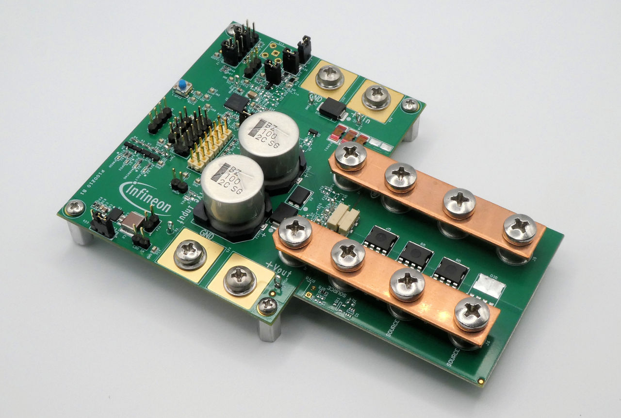
EVAL_XDP711-001
Content could not be loaded
Unfortunately, we were unable to load the content for this section. You may want to refresh the page or try again later.
製品仕様情報
-
Pout 範囲0 kW~6.6 kW
-
コンフィギュレーションXDP711-001, IPM018N10NM5LF2
-
ファミリーProtection and monitoring ICs
-
ボードタイプEvaluation Board
-
ボード名EVAL_XDP711-001
-
入力タイプDC
-
出力電圧 範囲7 V~80 V
-
出力電流 (最大)100 A
-
実装Stand Offs
-
対象アプリケーションServer factories, SMPS Switch Mode Power Supply, GPU accelerator cards, AI
-
認定Industrial
-
説明This board features the XDP711-001, a wide input voltage range (7V to 80V) hot-swap controller to provide controlled turn-on of the FETs to reduce the inrush current on capacitive load. It allows for testing of controlled turn-on of N-Channel MOSFETs in various footprints with option to add multiple FETs in parallel for higher power levels.
-
電源電圧 範囲7 V~80 V
| 推奨 | ||
|
OPN
|
EVALXDP711001TOBO1 | |
| 製品ステータス | active and preferred | |
| インフィニオン パッケージ | -- | |
| パッケージ名 | N/A | |
| 梱包サイズ | 1 | |
| 梱包形態 | CONTAINER | |
| MSL (湿度感受性レベル) | N/A | |
| 防湿梱包 | NON DRY | |
| 鉛フリー | No | |
| ハロゲンフリー | No | |
| RoHS対応 | Yes | |
|
Infineon stock last updated:
|
||
|
|
||
|
|
| 製品ステータス |
Active
|
|---|---|
| インフィニオン パッケージ | -- |
| パッケージ名 | - |
| 梱包サイズ | 1 |
| 梱包形態 | CONTAINER |
| MSL (湿度感受性レベル) | - |
| 防湿梱包 | NON DRY |
| 鉛フリー | |
| ハロゲンフリー | |
| RoHS準拠 | |
特長
- Easy input and output connections
- Provides PMBus® interface
- Per pin diagnostics
- Wide input voltage range
- On board capacitive load
- Fault, warning, power good LEDs
- RESTART push button
- Easy-mode-selection using jumpers
- Configurable 3.3 V / 5 V bias
利点
- Various MOSFET package selection
- Easy paralleling of MOSFET
- Easy-to-scale design with multiple shunts
- Port of XDP™ designer dongle
- Easy mode configuration
- Easy device address selection
- Board optimized for high-power designs
- On board I2C pullups
アプリケーション
Bill of Material
Share in WeChat
Scan the QR code with your WeChat App to share this page.