- ASIC
- バッテリー マネージメントIC
- クロックとタイミングソリューション
- ESDおよびサージ保護デバイス
- 自動車用イーサネット
- 評価ボード
- 高信頼性(HiRel)
- アイソレーター
- メモリ
- マイクロコントローラー
- パワー
- RF
- セキュリティ ソリューションおよびスマートカードソリューション
- センサー技術
- 小信号トランジスタおよびダイオード
- トランシーバー
- ユニバーサル シリアル バス(USB)
- ワイヤレス接続
- Search Tools
- Technology
- Packages
- Product Information
- Where to Buy
- 概要
- 自動車用イーサネットブリッジ
- 車載ネットワーク向け自動車用イーサネットPHY
- 車載ネットワーク向け自動車用イーサネット スイッチ
- 概要
- 組込みフラッシュIPソリューション
- フラッシュプラスRAM MCPソリューション
- F-RAM (強誘電体RAM)
- NORフラッシュ
- nvSRAM (不揮発性 SRAM)
- PSRAM (擬似スタティック RAM)
- 耐放射線・高信頼性メモリ
- RRAM抵抗RAM
- SRAM (スタティック RAM)
- ウェーハおよびダイメモリソリューション
- 概要
- 32ビットFM Arm® Cortex® マイクロコントローラー
- 32ビットAURIX™ TriCore™マイクロコントローラー
- 32ビットPSOC™ Arm® Cortex® マイクロコントローラー
- 32ビット TRAVEO™ T2G Arm® Cortex® マイクロコントローラー
- 32ビットXMC™産業用マイクロコントローラー Arm® Cortex®-M
- レガシー マイクロコントローラー
- MOTIX™マイクロコントローラー |Arm® Cortex®-Mベースの32ビット モーターコントロールSoC
- センシングコントローラー
- 概要
- AC-DC電力変換
- 従来型の車載パワートレインIC
- クラスD オーディオアンプIC
- 非接触パワー&センシングIC
- DC/DCコンバーター
- ダイオードとサイリスタ (Si/SiC)
- 窒化ガリウム(GaN)
- ゲートドライバIC
- IGBT – 絶縁ゲート型バイポーラトランジスタ
- インテリジェント パワーモジュール (IPM)
- LEDドライバIC
- モーター制御IC
- パワーMOSFET
- パワーモジュール
- 電源IC
- 保護および監視IC
- シリコンカーバイド (SiC)
- スマート パワー スイッチ
- ソリッドステートリレー (SSR)
- ワイヤレス充電IC
- 概要
- アンテナクロススイッチ
- アンテナチューナー
- バイアスと制御
- カプラ
- ドライバアンプ
- 高信頼性ディスクリート
- ローノイズアンプ (LNA)
- 高周波ダイオード
- RFスイッチ
- RFトランジスタ
- ワイヤレス制御向けレシーバー
- 概要
- Calypso®製品
- CIPURSE™ 製品
- 非接触メモリ
- OPTIGA™の組込みセキュリティ ソリューションの詳細
- SECORA™セキュリティソリューション
- セキュリ ティコントローラー
- スマートカードモジュール
- 政府ID向けスマートソリューション
- 概要
- USB 2.0 ペリフェラル コントローラー
- USB 3.2 ペリフェラル コントローラー
- USB ハブ コントローラー
- USB PD高電圧マイクロコントローラー
- USB-C AC-DC および DC-DC 充電ソリューション
- USB-C充電ポートコントローラー
- USB-Cパワーデリバリー コントローラー
- 概要
- AIROC™ オートモーティブワイヤレス
- AIROC™ Bluetooth®およびマルチプロトコル
- AIROC™ コネクトテッドMCU
- AIROC™ Wi-Fi + Bluetooth®コンボ
- 概要
- FM0+ 32ビット Arm® Cortex®-M0+ マイクロコントローラー (MCU)
-
FM3 32ビットArm® Cortex-M3®マイクロコントローラー (MCU) ファミリー
- 概要
- FM3 CY9AFx1xKシリーズ Arm® Cortex®-M3マイクロコントローラー (MCU)
- FM3 CY9AFx1xL/M/N シリーズ Arm® Cortex®-M3マイクロコントローラー (MCU)
- FM3 CY9AFx2xK/L シリーズ Arm® Cortex®-M3マイクロコントローラー (MCU)
- FM3 CY9AFx3xK/L シリーズ 超低リーク Arm® Cortex®-M3マイクロコントローラー (MCU)
- FM3 CY9AFx4xL/M/N シリーズ 低消費電力 Arm® Cortex®-M3マイクロコントローラー (MCU)
- FM3 CY9AFx5xM/N/Rシリーズ 低消費電力 Arm® Cortex®-M3マイクロコントローラー (MCU)
- FM3 CY9AFxAxL/M/N シリーズ 超低リーク Arm® Cortex®-M3 マイクロコントローラー (MCU)
- FM3 CY9BFx1xN/R 高性能シリーズ Arm® Cortex®-M3マイクロコントローラー (MCU)
- FM3 CY9BFx1xS/T 高性能シリーズ Arm® Cortex®-M3マイクロコントローラー (MCU)
- FM3 CY9BFx2xJシリーズ Arm® Cortex®-M3マイクロコントローラー (MCU)
- FM3 CY9BFx2xK/L/Mシリーズ Arm® Cortex®-M3マイクロコントローラー (MCU)
- FM3 CY9BFx2xS/Tシリーズ Arm® Cortex®-M3マイクロコントローラー (MCU)
- FM4 32ビットArm® Cortex-M4®マイクロコントローラー (MCU) ファミリー
- 概要
-
32 ビット TriCore™ AURIX™ – TC2x
- 概要
- AURIX™ ファミリー – TC21xL
- AURIX™ファミリー – TC21xSC (ワイヤレス充電)
- AURIX™ ファミリー – TC22xL
- AURIX™ ファミリー – TC23xL
- AURIX™ ファミリー – TC23xLA (ADAS)
- AURIX™ ファミリー – TC23xLX
- AURIX™ ファミリー – TC264DA (ADAS)
- AURIX™ ファミリー – TC26xD
- AURIX™ ファミリー – TC27xT
- AURIX™ ファミリー – TC297TA (ADAS)
- AURIX™ ファミリー – TC29xT
- AURIX™ファミリー – TC29xTT (ADAS)
- AURIX™ ファミリー – TC29xTX
- AURIX™ TC2xx (エミュレーションデバイス)
-
32 ビット TriCore™ AURIX™ – TC3x
- 概要
- AURIX™ ファミリー TC32xLP
- AURIX™ ファミリー – TC33xDA
- AURIX™ ファミリー - TC33xLP
- AURIX™ ファミリー – TC35xTA (ADAS)
- AURIX™ ファミリー – TC36xDP
- AURIX™ ファミリー – TC37xTP
- AURIX™ ファミリー – TC37xTX
- AURIX™ ファミリー – TC38xQP
- AURIX™ ファミリー – TC39xXA (ADAS)
- AURIX™ ファミリー – TC39xXX
- AURIX™ ファミリー – TC3Ex
- AURIX™ TC37xTE (エミュレーションデバイス)
- AURIX™ TC39xXE (エミュレーションデバイス)
- 32 ビット TriCore™ AURIX™ - TC4x
- 概要
- PSOC™ 4 Arm® Cortex® -M0/M0+
- PSOC™ 4 HV Arm® Cortex® -M0+
- PSOC™ 5 LP Arm® Cortex® -M3
- PSOC™ 6 Arm® Cortex®-M4 / M0+
- PSOC™マルチタッチArm® Cortex® -M0
- 32-bit PSOC™ Control Arm® Cortex®-M33 MCU
- 32ビットPSOC™フィンガープリントArm® Cortex®-M0+
- 自動車用PSOC™ 4 Arm® Cortex®-M0/M0+
- PSOC™ Edge Arm® Cortex® M55/M33
- 概要
- ボディ用32ビットTRAVEO™T2G Arm® Cortex®
- クラスター用の 32 ビット TRAVEO™ T2G Arm® Cortex®
- 概要
- 32ビットXMC1000産業用マイクロコントローラー Arm® Cortex®-M0
- Cortex-M4® Arm® 32ビットXMC4000産業用マイクロコントローラー
- XMC5000産業用マイクロコントローラーArm® Cortex® -M4F
- 32ビットXMC7000産業用マイクロコントローラー Arm® Cortex®-M7®
- 概要
- 整流ブリッジおよびACスイッチ
- CoolSiC™ ショットキーダイオード
- ダイオードベアダイ
- Si ダイオード
- サイリスタ/ダイオード パワーモジュール
- サイリスタソフトスタータモジュール
- サイリスタ / ダイオードディスク
- 概要
- 32-bit PSOC™ Control Arm® Cortex®-M33 MCU
- iMOTION™統合モーター制御ソリューション
- MOTIX™ MCU | Arm® Cortex®-Mベースの32ビット モーターコントロールSoC
- BLDCモーター用MOTIX™モーターゲートドライバIC
- ブラシ付きDCモーター用MOTIX™モーター制御IC
- サーボモーターおよびステッピングモーター用のMOTIX™マルチハーフブリッジIC
- 概要
- 車載用MOSFET
- デュアルMOSFET
- MOSFET(Si&SiC)モジュール
- NチャネルデプレッションモードMOSFET
- NチャネルパワーMOSFET
- PチャネルパワーMOSFET
- CoolSiC™ MOSFET
- 小信号/小電力MOSFET
- 概要
- 車載用トランシーバー
- OPTIREG™リニア電圧レギュレーター (LDO)
- OPTIREG™ PMIC
- OPTIREG™ スイッチャー(車載用)
- OPTIREG™ システム ベーシス チップ (SBC)
- 概要
- eFuse
-
ハイサイドスイッチ
- 概要
- Classic PROFET™ 12V |車載用スマート ハイサイドスイッチ
- Classic PROFET™ 24 V |車載用スマート ハイサイドスイッチ
- Power PROFET™ + 12/24/48 V |車載用スマート ハイサイドスイッチ
- PROFET™+ 12V |車載用スマート ハイサイドスイッチ
- PROFET™+ 24V |車載用スマート ハイサイドスイッチ
- PROFET™+ 48 V |車載用スマート ハイサイドスイッチ
- PROFET™+2 12V |車載用スマート ハイサイドスイッチ
- PROFET™ | 産業用スマート ハイサイドスイッチ
- PROFET™ Load Guard 12 V |車載用スマート ハイサイドスイッチ
- PROFET™ Wire Guard 12V | Automotive eFuse
- ローサイドスイッチ
- マルチチャネルSPIスイッチおよびコントローラー
- 概要
- EZ-USB™ CX3 MIPI CSI-2 to USB 5 Gbps カメラ コントローラー
- EZ-USB™ FX10 & FX5N USB 10Gbpsペリフェラルコントローラ
- EZ-USB™ FX20 USB 20 Gbpsペリフェラルコントローラー
- EZ-USB™ FX3 USB 5 Gbps ペリフェラル コントローラー
- EZ-USB™ FX3S USB 5 Gbps ペリフェラル コントローラー (ストレージ インターフェース付き)
- EZ-USB™ FX5 USB 5 Gbpsペリフェラルコントローラー
- EZ-USB™ SD3 USB 5 Gbps ストレージコントローラー
- EZ-USB™ SX3: FIFOインターフェースの USB 5 Gbps ペリフェラル コントローラー
- 概要
- EZ-PD™ CCG3 USB Type-Cポート コントローラーPD
- EZ-PD™ CCG3PA USB-C および PD
- EZ-PD™ CCG3PA-NFET USB-C PD コントローラー
- EZ-PD™ CCG7x シングルポート USB-Cパワーデリバリーおよび DC-DC コントローラー
- EZ-PD™ PAG1: 第 1 世代電源アダプター
- EZ-PD™ PAG2: 第 2 世代電源アダプター
- EZ-PD™ PAG2-PD USB-C PD コントローラー
- 概要
- EZ-PD™ ACG1F 1ポートUSB-Cコントローラー
- EZ-PD™ CCG2 USB Type-Cポート コントローラー
- EZ-PD™ CCG3PA車載用USB-Cおよびパワーデリバリーコントローラー
- EZ-PD™ CCG4 2 ポートUSB-CおよびPD
- EZ-PD™ CCG5デュアルポートおよび CCG5C シングルポート USB-C PDコントローラー
- EZ-PD™ CCG6 1ポート USB-C & PDコントローラー
- EZ-PD™ CCG6_CFP および EZ-PD™ CCG8_CFPデュアルシングルポート USB-C PD
- EZ-PD™ CCG6DFデュアルポートおよびCCG6SFシングルポートUSB-C PDコントローラー
- EZ-PD™ CCG7D車載用デュアルポートUSB-C PD + DC-DCコントローラー
- DC-DCコントローラーを搭載した、EZ-PD™ CCG7S車載用シングルポートUSB-C PDソリューション
- EZ-PD™ CCG7SAF車載用シングルポートUSB-C PD + DC-DCコントローラー + FET
- EZ-PD™ CCG8デュアル シングル ポートUSB-C PD
- EZ-PD™ CMG1 USB-C EMCAコントローラー
- 拡張パワーレンジ (EPR) 搭載EZ-PD™ CMG2 USB-C EMCA
- 最新情報
- 航空宇宙および防衛
- 自動車
- 民生用電子機器
- ヘルスケアとライフスタイル
- 家電製品
- 産業用アプリケーション
- 情報通信技術
- 再生可能エネルギー
- ロボティックス
- セキュリティソリューション
- スマートホームとスマートビルディング
- ソリューション
- 概要
- アダプターおよび充電器
- スマートテレビ向けの完全なシステムソリューション
- モバイルデバイスとスマートフォンソリューション
- マルチコプターとドローン
- 電動工具
- ホームエンターテインメント アプリケーション向けの半導体ソリューション
- スマート会議システム
- 概要
- アダプターおよび充電器
- 資産管理の追跡
- バッテリーの形成とテスト
- 電動フォークリフト
- バッテリー蓄電 (BESS)
- EV充電
- 高電圧ソリッドステート配電
- 産業用オートメーション
- 産業用モータードライブおよび制御
- インダストリー4.0向けの産業用ロボットシステムソリューション
- LED 照明システムの設計
- 小型電気自動車ソリューション
- 電動工具
- 送配電
- トラクション
- 無停電電源装置 (UPS)
- 概要
- データセンターおよびAIデータセンターソリューション
- エッジサーバーソリューション
- 通信インフラ
- Machine Learning Edge AI
- 概要
- デバイス認証とブランド保護
- モノのインターネット (IoT) 向けの組み込みセキュリティ
- eSIM アプリケーション
- 公的身分証明書
- モバイルセキュリティ
- 決済ソリューション
- アクセス管理および発券ソリューション
- 概要
- 家庭用ロボット
- 空調システム (HVAC)
- ホームオートメーションとビルオートメーション
- PCアクセサリ
- ホームエンターテインメント アプリケーション向けの半導体ソリューション
- 概要
- 車載用補助システム
- 車載ゲートウェイ
- 車載用パワー分配システム
- ボディコントロールモジュール(BCM)
- コンフォート&コンビニエンス エレクトロニクス
- ゾーンDC-DCコンバーター 48 V~12 V
- ゾーンコントロールユニット
- 概要
- アクティブサスペンションコントロール
- エアバッグシステム
- 車載用ブレーキング ソリューション
- 車載用ステアリング ソリューション
- シャーシ ドメイン制御
- リバーシブル シートベルト プリテンショナー
- 最新情報
- デジタル ドキュメンテーション
- 評価ボード
- ファインダー & セレクション ツール
- プラットフォーム
- サービス
- インフィニオン オンライン パワー シミュレーション プラットフォーム
- ソフトウェア
- ツール
- パートナー
- インフィニオン フォー メーカーズ
- ユニバーシティ アライアンス プログラム
- 概要
- AIROC™ ソフトウェアとツール
- AURIX™のツールとソフトウェア
- 自動車ソフトウェア開発用のDRIVECORE
- iMOTION™ ツールとソフトウェア
- インフィニオンのスマートパワースイッチおよびゲートドライバ ツールスイート
- MOTIX™ ソフトウェア&ツール
- OPTIGA™ ツールとソフトウェア
- PSOC™ ソフトウェアとツール
- TRAVEO™ ソフトウェアとツール
- XENSIV™ツールおよびソフトウェア
- XMC™ ツールとソフトウェア
- 概要
- AURIX™認証
- AURIX™開発ツール
- AURIX™組込みソフトウェア
- AURIX™マイクロコントローラーキット
- 概要
- OPTIGA™ TPMを使ってみる
- OPTIGA™開発ツール
- OPTIGA™組込みソフトウェア
- OPTIGA™ Trust証明書
- 概要
- CAPSENSE™コントローラー コンフィギュレーション ツール EZ-Click
- DC-DC統合POL電圧レギュレーター設定ツール – PowIRCenter
- EZ-USB™ SX3コンフィギュレーション ユーティリティ
- FM+ コンフィギュレーション ツール
- FMx設定ツール
- トランシーバーICコンフィギュレーション ツール
- USB EZ-PD™コンフィギュレーション ユーティリティ
- USB EZ-PD™コンフィギュレーション ユーティリティ
- USB EZ-USB™ HX3C Blaster Plusコンフィギュレーション ユーティリティ
- USB UARTコンフィギュレーション ユーティリティ
- XENSIV™タイヤ空気圧センサーのプログラミング
- 概要
- EZ-PD™ CCGx Dock ソフトウェア開発キット
- FMx Softune IDE
- ModusToolbox™ ソフトウェア
- PSOC™ ソフトウェア
- レーダー開発キット
- 錆
- USBコントローラーSDK
- ワイヤレス接続 Bluetooth メッシュヘルパー アプリケーション
- XMC™ DAVE™ソフトウェア
- 概要
- AIROC™ Bluetooth® Connect Appアーカイブ
- Cypress™ Programmerのアーカイブ
- EZ-PD™ CCGx 電力ソフトウェア開発キットのアーカイブ
- ModusToolbox™ ソフトウェアのアーカイブ
- PSOC™ Creatorのアーカイブ
- PSOC™ Designerのアーカイブ
- PSOC™ Programmerのアーカイブ
- USB EZ-PD™コンフィギュレーション ユーティリティ アーカイブ
- USB EZ-PD™ホストSDKのアーカイブ
- USB EZ-USB™ FX3のアーカイブ
- EZ-USB™ HX3PD コンフィギュレーション ユーティリティ
- WICED™ Smart SDKのアーカイブ
- WICED™ Studioのアーカイブ
- 最新情報
- サポート
- トレーニング
- 開発者コミュニティ
- News
ビジネス&財務プレス
16/12/2025
ビジネス&財務プレス
15/12/2025
ビジネス&財務プレス
09/12/2025
ビジネス&財務プレス
05/12/2025
- 会社概要
- 私たちのストーリー
- イベント
- プレス
- 投資家向け情報
- 採用情報
- 品質
- 最新ニュース
ビジネス&財務プレス
16/12/2025
ビジネス&財務プレス
15/12/2025
ビジネス&財務プレス
09/12/2025
ビジネス&財務プレス
05/12/2025
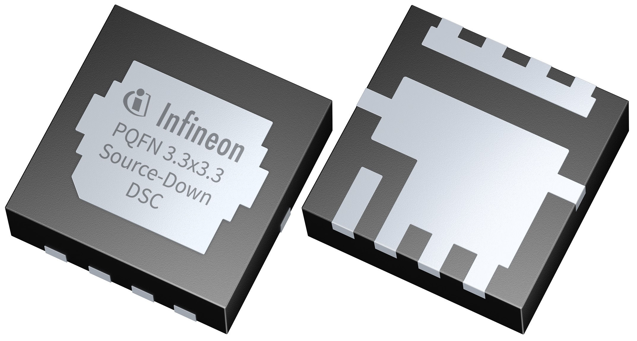
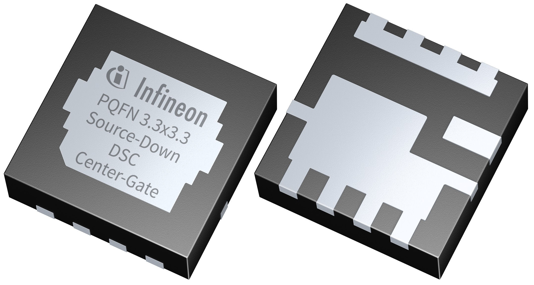
インフィニオン、PQFNデュアルサイド クーリング25-150VポートフォリオがOptiMOS™ソースダウン パワーMOSFETファミリーに登場
マーケットニュース
2022年12月15日、ミュンヘン (ドイツ)
将来のパワー エレクトロニクス システムの設計は、最先端の性能と電力密度の向上を継続的に推し進めています。この流れをサポートするため、インフィニオン テクノロジーズ (FSE: IFX / OTCQX: IFNNY) は、ボトムサイド (BSC) およびデュアルサイド クーリング (DSC) のバリエーションを持つ25-150 Vクラスの新しいソースダウン3.3 x 3.3 mm² PQFN製品ファミリーを発表します。この新製品ファミリーは、DC-DC電力変換において魅力的なソリューションを提供するためにコンポーネント レベルで大幅な機能強化を図っており、 サーバー、 通信インフラ、OR-ing、 バッテリー保護、 パワーツール、充電器といったアプリケーションにおけるシステム革新の可能性を切り開くものとなっています。
この新しいポートフォリオは、インフィニオンの最新のMOSFET技術と最先端のパッケージングを組み合わせ、システム性能を次のレベルに引き上げるものです。ソースダウン (SD) コンセプトでは、MOSFETダイのソース コンタクトがパッケージのフットプリント側に反転され、その後PCBにはんだ付けされます。さらに、このコンセプトは、ドレイン コンタクトのためにチップ上部のクリップ デザインを改良し、市場をリードするチップ対パッケージの面積比を実現しています。
システムの小型化が進む中、電力損失の低減と最適な熱管理という2つの重要なポイントがあります。クラス最高のPQFN 3.3 x 3.3 m²ドレインダウン デバイスと比較して、新しいファミリーはオン抵抗 (RDS (on) ) を最大25%と大幅に低減しました。インフィニオンのデュアルサイド クーリング搭載OptiMOS™ソースダウンPQFNは、熱インターフェースを強化し、スイッチからの電力損失をヒートシンクに向けさせることができます。デュアルサイド クーリングは、電源スイッチをヒートシンクに接続する最も直接的な方法を提供し、対応するソースダウン構造のボトムサイド クーリングと比較して、最大3倍まで電力許容損失量を向上させることができます。
フットプリントの異なる2つのバリエーションがあり、PCBの配線に高い柔軟性を提供します。従来のスタンダードゲート版は、既存のドレインダウン設計を迅速かつ容易に変更することができます。また、センターゲート (CG) 版は、ドライバーとゲートの接続を可能な限り短くするためにデバイスを並列化する新しい可能性を提供します。最大298Aという優れた連続電流性能を持つOptiMOS™ソースダウンPQFN 3.3 x 3.3 mm² 25-150V製品ファミリーは、最高のシステム性能を実現します。
供給体制について
OptiMOS™ソースダウンPQFN 3.3 x 3.3 mm² 25-150V製品ファミリーは、スタンダードゲート版とセンターゲート版の2つのバリエーションがあります。両製品ともデュアルサイド クーリング パッケージで、現在、注文を受け付けています。より詳細な情報は、 こちらで入手できます。
インフィニオンのエネルギー効率への貢献に関する詳細情報は、 こちら。
Press Photos
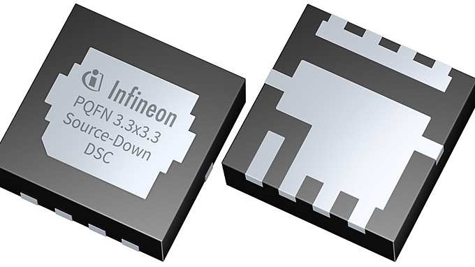
OptiMOS Source-Down DSC WHSON
Infineon’s OptiMOS Source-Down PQFN 3.3 x 3.3 mm² 25-150 V product family includes two footprint versions, Standard- and Center-Gate. Compared to best-in-class PQFN 3.3 x 3.3 m² Drain-Down devices, the new family significantly improves the on-resistance (RDS(on)) by up to 35 percent. With a Dual-Side Cooling package it provides an enhanced thermal interface to redirect power losses from the switch towards the heatsink increasing power dissipation capability by a factor of up to three compared to the corresponding Bottom-Side Cooled Source-Down variant.
JPEG
2146x1149 px
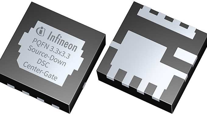
OptiMOS Source-Down DSC WHTFN
Infineon’s OptiMOS Source-Down PQFN 3.3 x 3.3 mm² 25-150 V product family includes two footprint versions, Standard- and Center-Gate. Compared to best-in-class PQFN 3.3 x 3.3 m² Drain-Down devices, the new family significantly improves the on-resistance (RDS(on)) by up to 35 percent. With a Dual-Side Cooling package it provides an enhanced thermal interface to redirect power losses from the switch towards the heatsink increasing power dissipation capability by a factor of up to three compared to the corresponding Bottom-Side Cooled Source-Down variant.
JPEG
2156x1149 px
Information Number : INFPSS202212-039j