
- ASIC
- Battery management ICs
- Clocks and timing solutions
- ESD and surge protection devices
- Automotive Ethernet
- Evaluation Boards
- High reliability
- Isolation
- Memories
- Microcontroller
- Power
- RF
- Security and smart card solutions
- Sensor technology
- Small signal transistors and diodes
- Transceivers
- Universal Serial Bus (USB)
- Wireless connectivity
- Search Tools
- Technology
- Packages
- Product Information
- Ordering
- Overview
- Automotive Ethernet PHY for in-vehicle networking
- Automotive Ethernet Switches for in-vehicle networking
- Overview
- Embedded flash IP solutions
- Flash+RAM MCP solutions
- F-RAM (Ferroelectric RAM)
- NOR flash
- nvSRAM (non-volatile SRAM)
- PSRAM – Pseudostatic RAM
- Radiation hardened and high-reliability memories
- SRAMs (Static Random Access Memory)
- Wafer and die memory solutions
- Overview
- AURIX™ TriCore™ MCUs
- PSOC™ MCUs
- TRAVEO™ T2G MCUs
- XMC™ MCUs
- Legacy MCUs
- MOTIX™ motor control SoCs/SIPs
- Overview
- AC-DC power conversion
- Automotive conventional powertrain ICs
- Class D audio amplifier ICs
- Contactless power and sensing ICs
- DC-DC converters
- Diodes and thyristors (Si/SiC)
- eFuses
- Gallium nitride (GaN)
- Gate Driver ICs
- IGBTs – Insulated gate bipolar transistors
- Intelligent power modules (IPM)
- JFETs
- LED driver ICs
- Motor drivers
- MOSFETs
- Power modules
- Power supply ICs
- Protection and monitoring ICs
- Silicon carbide (SiC)
- Smart power switches
- Solid state relays and isolators
- Wireless charging ICs
- Overview
- Antenna cross switches
- Antenna tuners
- Bias and control
- Coupler
- Driver amplifiers
- Rad hard microwave and RF
- Low noise amplifiers (LNAs)
- RF diode
- RF switches
- RF transistors
- Wireless control receiver
- Overview
- Calypso® products
- CIPURSE™ products
- Contactless memories
- OPTIGA™ embedded security solutions
- SECORA™ security solutions
- Security controllers
- Smart card modules
- Smart solutions for government ID
- Overview
- ToF 3D image sensors
- Current sensors
- Gas sensors
- Inductive position sensors
- MEMS microphones
- Pressure sensors
- Radar sensors
- Magnetic position sensors
- Magnetic speed sensors
- Capacitive sensors
- Temperature sensors
- Battery sensors
- Digital X-ray
- Computed tomography
- Sensor interface ASICs
- Overview
- Bipolar transistors
- Diodes
- Small signal/small power MOSFET
- Overview
- Automotive transceivers
- Control communication
- Powerline communications
- Overview
- USB 2.0 peripheral controllers
- USB 3.2 peripheral controllers
- USB hub controllers
- USB PD high-voltage microcontrollers
- USB-C AC-DC and DC-DC charging solutions
- USB-C charging port controllers
- USB-C Power Delivery controllers
- Overview
- AIROC™ Automotive wireless
- AIROC™ Bluetooth® and multiprotocol
- AIROC™ connected MCU
- AIROC™ Wi-Fi + Bluetooth® combos
- AIROC™ Ultra-Wide Band Solutions
- Overview
- Commercial off-the-shelf (COTs) memory portfolio
- Defense memory portfolio
- High-reliability power conversion and management
- Overview
- Rad hard microwave and RF
- Radiation hardened power
- Space memory portfolio
- Overview
- Parallel NOR flash
- SEMPER™ NOR flash family
- SEMPER™ X1 LPDDR flash
- Serial NOR flash
- Overview
-
32-bit TriCore™ AURIX™ – TC2x
- Overview
- AURIX™ family – TC21xL
- AURIX™ family – TC21xSC (wireless charging)
- AURIX™ family – TC22xL
- AURIX™ family – TC23xL
- AURIX™ family – TC23xLA (ADAS)
- AURIX™ family – TC23xLX
- AURIX™ family – TC264DA (ADAS)
- AURIX™ family – TC26xD
- AURIX™ family – TC27xT
- AURIX™ family – TC297TA (ADAS)
- AURIX™ family – TC29xT
- AURIX™ family – TC29xTT (ADAS)
- AURIX™ family – TC29xTX
- AURIX™ TC2x emulation devices
-
32-bit TriCore™ AURIX™ – TC3x
- Overview
- AURIX™ family - TC32xLP
- AURIX™ family – TC33xDA
- AURIX™ family - TC33xLP
- AURIX™ family – TC35xTA (ADAS)
- AURIX™ family – TC36xDP
- AURIX™ family – TC37xTP
- AURIX™ family – TC37xTX
- AURIX™ family – TC38xQP
- AURIX™ family – TC39xXA (ADAS)
- AURIX™ family - TC39xXX/XP
- AURIX™ family – TC3Ex
- AURIX™ TC37xTE (emulation devices)
- AURIX™ TC39xXE (emulation devices)
- 32-bit TriCore™ AURIX™ – TC4x
- Overview
- PSOC™ 4 Microcontroller: Arm® Cortex®-M0/M0+
- PSOC™ 4 HV Arm® Cortex®-M0+
- PSOC™ 5 LP Arm® Cortex®-M3
- PSOC™ 6 Arm® Cortex®-M4/M0+
- PSOC™ Multitouch Touchscreen Controller
- PSOC™ Control C3 Arm® Cortex®-M33
- PSOC™ Automotive 4: Arm® Cortex®-M0/M0+
- PSOC™ Edge Arm® Cortex® M55/M33
- PSOC™ Control C1 Arm® Cortex®-M0
- Overview
- 32-bit TRAVEO™ T2G Arm® Cortex® for body
- 32-bit TRAVEO™ T2G Arm® Cortex® for cluster
- Overview
- 32-bit XMC1000 industrial microcontroller Arm® Cortex®-M0
- 32-bit XMC4000 industrial microcontroller Arm® Cortex®-M4
- XMC5000 Industrial Microcontroller Arm® Cortex®-M4F
- 32-bit XMC7000 Industrial Microcontroller Arm® Cortex®-M7
- Overview
- Legacy 32-bit MCU
- Legacy 8-bit/16-bit microcontroller
- Other legacy MCUs
- 32-bit FM Arm® Cortex® Microcontroller
- Sensing controllers
- Overview
- AC-DC integrated power stage - CoolSET™
- AC-DC PWM and PFC controller
- Overview
- Bridge rectifiers & AC switches
- CoolSiC™ Schottky diodes
- Diode bare dies
- Silicon diodes
- Thyristor / Diode Power Modules
- Thyristor soft starter modules
- Thyristor/diode discs
- Overview
- GaN bidirectional switches
- GaN smart
- GaN transistors (GaN HEMTs)
- GaN with integrated driver
- GaN bare dies
- Overview
- Automotive gate driver ICs
- Gate Driver ICs for GaN HEMTs
- Gate Driver ICs for SiC MOSFETs
- Half-Bridge Gate Driver ICs
- High-Side Gate Driver ICs
- Isolated Gate Driver ICs
- Level-Shift Gate Driver ICs
- Low-Side Gate Driver ICs
- Three-Phase Gate Driver ICs
- Transformer Driver ICs
- Overview
- AC-DC LED driver ICs
- Ballast IC
- DC-DC LED driver IC
- LED dimming interface IC
- Linear LED driver IC
- LITIX™ - Automotive LED Driver IC
- NFC wireless configuration IC with PWM output
- VCSEL driver
- Overview
- BLDC motor drivers
- BDC motor drivers
- Stepper & servo motor drivers
- Motor drivers with MCU
- Bridge drivers with MOSFETs
- Gate Driver ICs
- Overview
- Automotive MOSFET: 30 V to 800 V
- Dual MOSFETs
- MOSFET (Si & SiC) Modules
- N-channel depletion mode MOSFET
- N-channel MOSFETs
- P-channel MOSFETs
-
Silicon carbide CoolSiC™ MOSFETs
- Overview
- Silicon Carbide MOSFET modules
- Silicon carbide MOSFET discretes
- Silicon carbide MOSFETs bare dies
- Silicon Carbide Bidirectional Switches
- 400 V / 440 V Silicon Carbide MOSFETs
- 650 V Silicon Carbide MOSFETs
- 750 V Silicon Carbide MOSFETs
- 1200 V Silicon Carbide MOSFETs
- 1700 V Silicon Carbide MOSFETs
- 2000 V Silicon Carbide MOSFETs
- 2300 V Silicon Carbide MOSFETs
- 3300 V Silicon Carbide MOSFETs
- Small signal/small power MOSFET
- Overview
- IGBT modules
- MOSFET (Si & SiC) Modules
- Intelligent power modules (IPM)
- Diodes and thyristors (Si/SiC)
- Automotive IGBT and CoolSiC™ MOSFET modules
- High density power modules
- Overview
- Automotive transceivers
- Linear voltage regulators
- Power management ICs (PMIC)
- Automotive switching regulators
- System Basis Chips (SBC)
- Overview
- High-side switches
- Low-side switches
- Multichannel SPI Switches & Controller
- Automotive eFuses
- Overview
- Radar sensors for automotive
- Radar sensors for IoT
- Overview
- EZ-USB™ CX3 MIPI CSI2 to USB 3.0 camera controller
- EZ-USB™ FX10 & FX5N USB 10Gbps peripheral controller
- EZ-USB™ FX20 USB 20 Gbps peripheral controller
- EZ-USB™ FX3 USB 5 Gbps peripheral controller
- EZ-USB™ FX3S USB 5 Gbps peripheral controller with storage interface
- EZ-USB™ FX5 USB 5 Gbps peripheral controller
- EZ-USB™ SD3 USB 5 Gbps storage controller
- EZ-USB™ SX3 FIFO to USB 5 Gbps peripheral controller
- Overview
- EZ-PD™ PMG1-B1 Battery Charge Controller with USB-C PD MCU
- EZ-PD™ PMG1-S0 high-voltage MCU with USB-C and PD
- EZ-PD™ PMG1-S1 high-voltage MCU with USB-C and PD
- EZ-PD™ PMG1-S2 high-voltage MCU with USB PD
- EZ-PD™ PMG1-S3 high-voltage MCU with USB-C & PD
- EZ-PD™ PMG1-B2 Battery Charge Controller with USB-C PD MCU
- Overview
- EZ-PD™ CCG3 USB type-C port controller PD
- EZ-PD™ CCG3PA USB-C and PD
- EZ-PD™ CCG3PA-NFET USB-C PD controller
- EZ-PD™ CCG7x consumer USB-C Power Delivery & DC-DC controller
- EZ-PD™ PAG1: power adapter generation 1
- EZ-PD™ PAG2: Power Adapter Generation 2
- EZ-PD™ PAG2-PD USB-C PD Controller
- Overview
- EZ-PD™ ACG1F one-port USB-C controller
- EZ-PD™ CCG2 USB Type-C port controller
- EZ-PD™ CCG3PA Automotive USB-C and Power Delivery controller
- EZ-PD™ CCG4 two-port USB-C and PD
- EZ-PD™ CCG5 dual-port and CCG5C single-port USB-C PD controllers
- EZ-PD™ CCG6 one-port USB-C & PD controller
- EZ-PD™ CCG6_CFP and EZ-PD™ CCG8_CFP Dual-Single-Port USB-C PD
- EZ-PD™ CCG6DF dual-port and CCG6SF single-port USB-C PD controllers
- EZ-PD™ CCG7D Automotive dual-port USB-C PD + DC-DC controller
- EZ-PD™ CCG7S Automotive single-port USB-C PD solution with a DC-DC controller + FETs
- EZ-PD™ CCG8 dual-single-port USB-C PD
- EZ-PD™ CMG1 USB-C EMCA controller
- EZ-PD™ CMG2 USB-C EMCA controller with EPR
Browse by core architecture
Browse by key technologies
Browse by design resources & partners
- LATEST IN
- Aerospace and defense
- AI and data center
- Automotive
- Communications
- Consumer electronics
- Industrial
- Security solutions
- Smart home and building
- Solutions
- Overview
- Defense applications
- Space applications
- Overview
- Data center power solutions
- Edge computing
- Machine Learning Edge AI
- Overview
- ADAS & autonomous driving
- Automotive body electronics
- Automotive LED lighting systems
- Automotive zonal architecture
- Chassis control & safety
- Electric vehicle drivetrain system
- EV thermal management system
- In-vehicle infotainment & HMI
- Light electric vehicle solutions
- Overview
- Satellite communications
- Telecommunications infrastructure
- Overview
- AR and smart glasses
- Complete system solutions for smart TVs
- Consumer Wearables
- Drones
- Home appliances
- Mobile device and smartphone solutions
- Photovoltaic
- Power adapters and chargers
- Semiconductor solutions for home entertainment applications
- Smart conference systems
- Overview
- Asset Tracking
- Battery energy storage (BESS)
- Battery formation and testing
- Digital health
- Electric forklifts
- EV charging
- High voltage solid-state power distribution
- Hydrogen electrolysis
- Industrial & Medical SMPS
- Industrial automation
- Industrial motor drives and controls
- Industrial robots
- LED lighting system design
- Light electric vehicle solutions
- Photovoltaic
- Power adapters and chargers
- Power tools
- Power transmission and distribution
- Robotics
- Traction
- Uninterruptible power supplies (UPS)
- Wind power
- Overview
- Access control and ticketing
- Device authentication and brand protection
- Embedded security for the Internet of Things (IoT)
- eSIM applications
- Government identification
- Mobile security
- Payment solutions
- Overview
- Domestic robots
- Heating ventilation and air conditioning (HVAC)
- Home and building automation
- PC accessories
- Semiconductor solutions for home entertainment applications
- Overview
- Battery management systems (BMS)
- Connectivity
- Human Machine Interface
- Machine Learning Edge AI
- Motor control
- Power conversion
- Security
- Sensor solutions
- System diagnostics and analytics
- Overview
- Data center power distribution
- FPGAs in datacenter applications
- Power system reliability modeling
-
Server rack power management
- Overview
- AI accelerator cards
- AMD CPU voltage regulator Ics
- Ampere CPU voltage regulator Ics
- Intel CPU voltage regulator Ics
- Intermediate Bus Converter (IBC)
- Network switches for AI data centers and server racks
- Server battery backup units (BBU)
- Server power path protection
- Server power supply units (PSU)
- SmartNIC cards
- Overview
- Automotive animated LED lighting system
- Automotive LED front single light functions
- Automotive LED rear single light functions
- Full LED headlight system - multi-channel LED driver
- LED driver solutions for electric two- and three-wheelers
- LED pixel light controller - supply & communication
- Static interior ambient LED light
- Overview
- Active suspension control
- Automotive braking solutions
- Automotive steering solutions
- Chassis domain control
- Overview
-
Automotive battery management system
- Overview
- Automotive battery cell monitoring & balancing
- Automotive battery control unit (BCU)
- Automotive battery isolated communication
- Automotive battery management system (BMS) - 12 V to 24 V
- Automotive battery management system (BMS) - 48 V
- Automotive battery management system (BMS) - high-voltage
- Automotive battery pack monitoring
- Automotive battery passport & event logging
- Automotive battery protection & disconnection
- Automotive current sensing & coulomb counting
- BMS (electric two- & three-wheelers)
- Auxiliary inverter
- Auxiliary inverter - high-voltage (commercial vehicles)
- DC-DC converter high-voltage
- DC-DC converter high-voltage (commercial vehicles)
- EV charging
- EV traction inverter
- FCEV powertrain solutions
- On-board charging (electric commercial vehicles)
- On-board charging (OBC)
- On-board charging (OBC) solutions for electric two- and three-wheelers
- Traction inverter (electric commercial vehicles)
- Traction inverter (electric two- & three-wheelers)
- Overview
- Audio amplifier solutions
- Complete system solutions for smart TVs
- Distribution audio amplifier unit solutions
- Home theater installation speaker system solutions
- Party speaker solutions
- PoE audio amplifier unit solutions
- Portable speaker solutions
- Powered active speaker systems
- Remote control
- Smart speaker designs
- Soundbar solutions
- Overview
- Disposable healthcare equipment
- Durable healthcare equipment
- Healthcare wearables
- Overview
- Data center power solutions
- Digital input/output (I/O) modules
- DIN rail power supply solutions
- Home and building automation
- Industrial HMI Monitors and Panels
- Industrial motor drives and controls
- Industrial PC
- Industrial robots
- Machine vision
- Mobile robots (AGV, AMR)
- Programmable logic controller (PLC)
- Solid-state circuit breaker (SSCB)
- Uninterruptible power supplies (UPS)
- Overview
- Automotive battery management system
- Industrial and consumer BMS
- Overview
- AC-DC power conversion
- DC-DC power conversion
- Overview
- Power supply health monitoring
- LATEST IN
- Digital documentation
- Boards & Kits
- Finder & selection tools
- Platforms
- Services
- Simulation & Modeling
- Software
- Tools
- Partners
- Infineon for Makers
- University Alliance Program
- Overview
- Bipolar Discs Finder
- Bipolar Module Finder
- Connected Secure Systems Finder
- Diode Rectifier Finder
- ESD Protection Finder
- Evaluation Board Finder
- Gate Driver Finder
- IGBT Discrete Finder
- IGBT Module Finder
- IPM Finder
- Microcontroller Finder
- MOSFET Finder
- PMIC Finder
- Product Finder
- PSOC™ and FMx MCU Board & Kit Finder
- Radar Finder
- Reference Design Finder
- Simulation Model Finder
- Smart Power Switch Finder
- Transceiver Finder
- Voltage Regulator Finder
- Wireless Connectivity Board & Kit Finder
- Infineon Gate Driver Recommendation Tool
- Overview
- AIROC™ software & tools
- AURIX™ software & tools
- DRIVECORE™ for automotive software development
- iMOTION™ software & tools
- Infineon Smart Power Switches & Gate Driver Tool Suite
- MOTIX™ software & tools
- OPTIGA™ software & tools
- PSOC™ software & tools
- TRAVEO™ software & tools
- XENSIV™ software & tools
- XMC™ software & tools
- Overview
- HiRel Fit Rate Tool
- Infineon Designer
- Interactive product sheet
- IPOSIM Online Power Simulation Platform
- InfineonSpice Offline Simulation Tool
- OPTIREG™ automotive power supply ICs Simulation Tool (PLECS)
- Power MOSFET Simulation Models
- PowerEsim Switch Mode Power Supply Design Tool
- Solution Finder
- XENSIV™ Magnetic Sensor Simulation Tool
- Overview
- Configuration
- Hardware Development
- Programming & Testing
- SDK
- Tools Archive
- Utilities
- Overview
- AURIX™ certifications
- AURIX™ development tools
-
AURIX™ Embedded Software
- Overview
- AURIX™ Applications software
- AURIX™ Artificial Intelligence
- AURIX™ Gateway
- AURIX™ iLLD Drivers
- Infineon safety
- AURIX™ Security
- AURIX™ TC3xx Motor Control Application Kit
- AURIX™ TC4x SW application architecture
- Infineon AUTOSAR
- Communication and Connectivity
- Middleware
- Non AUTOSAR OS/RTOS
- OTA
- AURIX™ Microcontroller Kits
- Overview
- TRAVEO™ Development Tools
- TRAVEO™ Embedded Software
- Overview
- XENSIV™ Development Tools
- XENSIV™ Embedded Software
- XENSIV™ evaluation boards
- Overview
- CAPSENSE™ Controllers Code Examples
- Memories for Embedded Systems Code Examples
- PSOC™ 1 Code Examples for PSOC™ Designer
- PSOC™ 3 Code Examples for PSOC™ Creator
- PSOC™ 3/4/5 Code Examples
- PSOC™ 4 Code Examples for PSOC™ Creator
- PSOC™ 6 Code Examples for PSOC™ Creator
- PSOC™ 63 Code Examples
- USB Controllers Code Examples
- Overview
- AIROC™ Wi-Fi & Bluetooth EZ-Serial Module Firmware Platform
- AIROC™ Wi-Fi & Bluetooth Linux and Android Drivers
- emWin Graphics Library and GUI for PSOC™
- Infineon Complex Device Driver for Battery Management Systems
- Memory Solutions Hub
- PSOC™ 6 Peripheral Driver Library (PDL) for PSOC™ Creator
- USB Controllers EZ-USB™ GX3 Software and Drivers
- Overview
- CAPSENSE™ Controllers Configuration Tools EZ-Click
- DC-DC Integrated POL Voltage Regulators Configuration Tool – PowIRCenter
- EZ-USB™ SX3 Configuration Utility
- FM+ Configuration Tools
- FMx Configuration Tools
- Tranceiver IC Configuration Tool
- USB EZ-PD™ Configuration Utility
- USB EZ-PD™ Dock Configuration Utility
- USB EZ-USB™ HX3C Blaster Plus Configuration Utility
- USB UART Config Utility
- XENSIV™ Tire Pressure Sensor Programming
- Overview
- EZ-PD™ CCGx Dock Software Development Kit
-
FMx Softune IDE
- Overview
- RealOS™ Real-Time Operating System
- Softune IDE Language tools
- Softune Workbench
- Tool Lineup for F2MC-16 Family SOFTUNE V3
- Tool Lineup for F2MC-8FX Family SOFTUNE V3
- Tool Lineup for FR Family SOFTUNE V6
- Virtual Starter Kit
- Windows 10 operation of released SOFTUNE product
- Windows 7 operation of released SOFTUNE product
- Windows 8 operation of released SOFTUNE product
- Infineon GUI Designer
- ModusToolbox™ Software
- PSOC™ Creator Software
- Radar Development Kit
- RUST
- USB Controllers SDK
- Wireless Connectivity Bluetooth Mesh Helper Applications
- XMC™ DAVE™ Software
- Overview
- AIROC™ Bluetooth® Connect App Archive
- Cypress™ Programmer Archive
- EZ-PD™ CCGx Power Software Development Kit Archive
- ModusToolbox™ Software Archive
- PSOC™ Creator Archive
- PSOC™ Designer Archive
- PSOC™ Programmer Archive
- USB EZ-PD™ Configuration Utility Archives
- USB EZ-PD™ Host SDK Archives
- USB EZ-USB™ FX3 Archive
- USB EZ-USB™ HX3PD Configuration Utility Archive
- WICED™ Smart SDK Archive
- WICED™ Studio Archive
- Overview
- Infineon Developer Center Launcher
- Infineon Register Viewer
- Pin and Code Wizard
- Timing Solutions
- Wireless Connectivity
- LATEST IN
- Support
- Training
- Developer Community
- News
Business & Financial Press
Oct 07, 2026
Business & Financial Press
Oct 05, 2026
Business & Financial Press
Oct 01, 2026
Business & Financial Press
Sep 29, 2026
- Company
- Our stories
- Events
- Press
- Investor
- Careers
- Quality
- Latest news
Business & Financial Press
Oct 07, 2026
Business & Financial Press
Oct 05, 2026
Business & Financial Press
Oct 01, 2026
Business & Financial Press
Sep 29, 2026
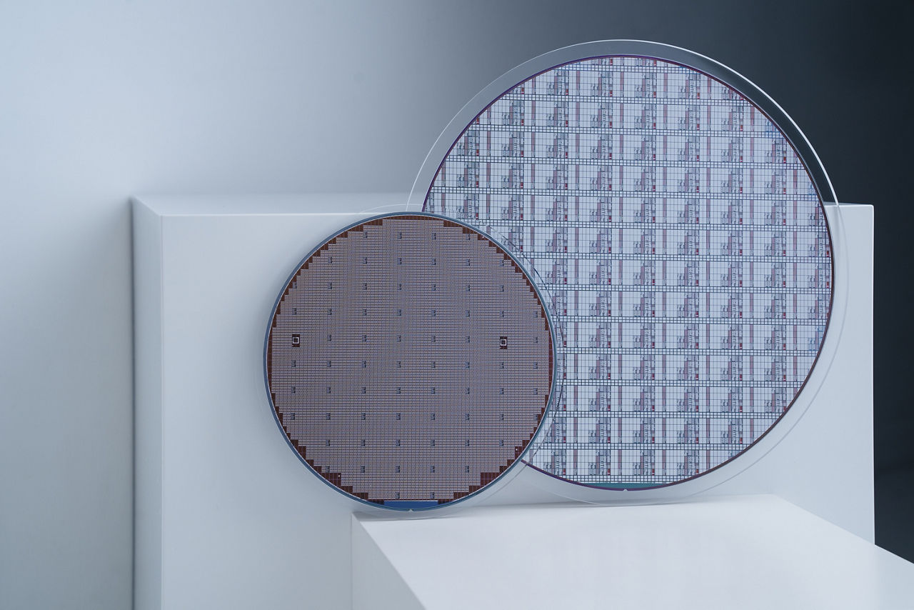
Gallium Nitride (GaN) is a wide-bandgap semiconductor material that enables smaller, faster, and more efficient power systems than conventional silicon technologies.
Thanks to its high switching speed, high power density, and low energy losses, GaN is increasingly used in electric vehicle charging systems, renewable energy solutions, AI data-center power supplies, RF communications, and industrial power electronics. These characteristics help designers develop more compact systems with improved energy efficiency and performance.
For over half a century, silicon has been the foundation of the semiconductor industry. However, as consumer and industrial demands push toward higher power densities, miniaturization, and faster switching speeds, traditional silicon is rapidly reaching its theoretical limitations. Enter Gallium Nitride (GaN). As a wide bandgap (WBG) semiconductor, GaN offers the next big step in a fundamentally superior matrix of physical properties.
GaN technology is the driving force behind the next industrial revolution in power electronics, radio frequency (RF) communications, and optoelectronics. From the ultra-compact fast chargers powering modern laptops and smartphones to the radar systems scanning global airspace and the universe, GaN is replacing legacy silicon due to its ability to conduct electrons faster, withstand higher electric fields, and operate at elevated temperatures. Furthermore, its unique optical properties enabled the creation of the blue light-emitting diode (LED), transforming modern lighting and optical storage.
Technology review explores the science of GaN, its extensive applications across multiple domains, and the distinct advantages that position it as the superior semiconductor technology of the future. As GaN devices mature, they are reshaping the electronics industry from the ground up.
Gallium Nitride is a chemical compound, specifically, it is a binary (two-element) compound made up of equal parts of the metallic element Gallium (Ga) and the gaseous element Nitrogen (N). Unlike Silicon (Si) or Germanium (Ge), which are pure, single-element semiconductors, GaN belongs to a class of materials called compound semiconductors — a category that also includes Gallium Arsenide (GaAs).
- The Power of Synergy: Separately, gallium is a soft metal that melts in your hand, and nitrogen is an invisible gas you breathe. Combined, they form an incredibly hard, rugged crystal with a melting point over 2,200°C (3,992°F).
- The "III-V" Classification: In chemistry, Gallium is from Group III of the periodic table, and Nitrogen is from Group V. Because of this, GaN is specifically known as a III-V compound semiconductor.
- Tunable Physics: Because it is a compound, scientists can mix in small amounts of other elements—like Aluminum (Al) or Indium (In)—to create variations like AlGaN or InGaN. This allows them to change the material's properties, altering the color of light it emits (from green to UV) or adjusting how much electrical voltage it can handle.
In nature, gallium and nitrogen do not easily combine on their own. Creating Gallium Nitride (GaN) requires precise, high-tech chemical manufacturing.
- Gallium (Ga): A post-transition metal with three electrons in its outer shell.
- Nitrogen (N): A non-metal gas with five electrons in its outer shell.
When brought together under extreme heat and pressure, gallium shares its three outer electrons with nitrogen. This creates a highly stable, tightly bound covalent crystal structure known as a Wurtzite crystal lattice.
Because nitrogen atoms are very small, they hold onto their electrons incredibly tightly. This tight grip creates a massive physical hurdle for electrons trying to break free, resulting in a wide bandgap (3.4 electron-volts). It takes three times more energy to move an electron through GaN than it does through traditional silicon.
Want to go deeper on the physics behind this? Read GaN Bandgap: What It Is and Why It Matters.
Because you cannot mine GaN out of the ground, scientists grow it. They use a process called Metalorganic Chemical Vapor Deposition (MOCVD).
- Gases containing gallium and nitrogen are pumped into a vacuum chamber.
- The chamber is heated to temperatures often exceeding 1,000°C (1,832°F).
- The gases chemically react, causing atoms of gallium and nitrogen to rain down and arrange themselves into a perfectly flat, atom-thick crystal layer onto a base substrate (usually silicon or sapphire).
Once this rugged crystal lattice is formed, its unique physics allow it to manipulate light and electricity in ways silicon never could, giving rise to the many GaN devices used across today's tech industries. This same manufacturing foundation underlies every category of GaN chips and GaN products on the market.
Curious how the substrate choice affects cost and performance? See GaN-on-Silicon and GaN-on-Silicon Carbide for Power Electronics: A Review.
- Gallium (Ga): A post-transition metal with three electrons in its outer shell.
- Nitrogen (N): A non-metal gas with five electrons in its outer shell.
When brought together under extreme heat and pressure, gallium shares its three outer electrons with nitrogen. This creates a highly stable, tightly bound covalent crystal structure known as a Wurtzite crystal lattice.
Because nitrogen atoms are very small, they hold onto their electrons incredibly tightly. This tight grip creates a massive physical hurdle for electrons trying to break free, resulting in a wide bandgap (3.4 electron-volts). It takes three times more energy to move an electron through GaN than it does through traditional silicon.
Want to go deeper on the physics behind this? Read GaN Bandgap: What It Is and Why It Matters.
Because you cannot mine GaN out of the ground, scientists grow it. They use a process called Metalorganic Chemical Vapor Deposition (MOCVD).
- Gases containing gallium and nitrogen are pumped into a vacuum chamber.
- The chamber is heated to temperatures often exceeding 1,000°C (1,832°F).
- The gases chemically react, causing atoms of gallium and nitrogen to rain down and arrange themselves into a perfectly flat, atom-thick crystal layer onto a base substrate (usually silicon or sapphire).
Once this rugged crystal lattice is formed, its unique physics allow it to manipulate light and electricity in ways silicon never could, giving rise to the many GaN devices used across today's tech industries. This same manufacturing foundation underlies every category of GaN chips and GaN products on the market.
Curious how the substrate choice affects cost and performance? See GaN-on-Silicon and GaN-on-Silicon Carbide for Power Electronics: A Review.
GaN technology has moved well beyond the lab, and today it touches nearly every corner of consumer electronics, high power applications, and the wider electronics industry.
Because GaN power transistors combine high power density with strong thermal performance, they increasingly outperform silicon transistors and other semiconductor devices built on conventional silicon, enabling more efficient power systems and smaller electronic devices.

High level GaN uses cases

Power use cases of GaN
It manipulates light (optoelectronics)
When an electric current passes through the gallium-nitrogen crystal lattice, electrons drop into "holes" in the structure and release their energy as light. Because the bandgap is so wide, that energy is packed into ultra-short, high-energy wavelengths.
- Blue and White LEDs: This exact wavelength produces brilliant blue light. By adding a yellow phosphor coating over a blue GaN LED, scientists created the bright, energy-efficient white LED bulbs that illuminate homes and smartphone screens globally today.
- Blue Lasers & Optical Storage: Concentrating this light in GaN laser diodes creates a blue laser beam. Because blue light wavelengths are much shorter than red light, lasers can read microscopic data packed tightly together, enabling Blu-ray discs and high-density optical archiving.
It creates an "electron highway" for GaN transistors and power ICs
When a layer of Aluminum Gallium Nitride (AlGaN) is placed on top of pure GaN, a fascinating quantum phenomenon occurs at the boundary. The atoms pull at each other, creating a natural, highly concentrated sheet of free-floating electrons called a Two-Dimensional Electron Gas (2DEG).
- Ultra-Fast Fast Chargers: This electron sheet has incredibly high mobility. Electrons can zoom through the material with almost zero resistance. This allows GaN transistors to switch on and off millions of times per second, letting power supplies (like phone and laptop chargers) convert electricity with minimal heat, shrinking their physical size by up to 70%.
- Data Center Power: Modern data centers and AI server farms require staggering amounts of electrical power. A massive portion of this energy is lost as heat during the step-down conversion from high-voltage AC/DC power to low-voltage DC power. By using GaN in data center power ICs, power supply units (PSUs), and DC-DC converters (also called intermediate bus converters (IBC)), operators can increase power efficiency, dramatically reduce the energy lost, and increase power density in their racks.
- Electric Vehicles (EVs): This same "highway" allows GaN to handle massive amounts of electrical power. EV makers use it in on-board chargers to convert grid power into battery power faster, saving space and reducing car weight.
It handles extreme frequencies (RF & telecommunications)
Because the gallium-nitrogen atomic bond is so tight, the material can withstand immense electrical stress (voltage) while operating at incredibly high frequencies (gigahertz range).
- 5G/6G Cellular Towers: Traditional silicon chips burn out or lose signal clarity at high frequencies. GaN-based power amplifiers can effortlessly push massive amounts of data through the air over long distances, serving as the backbone for 5G and emerging 6G infrastructure.
- Advanced Radar: Radars use hundreds of tiny GaN transmitters working together. Because GaN can transmit incredibly strong high-frequency signals, these radars can see much farther and track smaller targets with razor-sharp precision.
It resists radiation bombardment (space exploration)
The strong, tight chemical bond between gallium and nitrogen gives GaN an inherent, natural defense against space radiation. In deep space and Earth orbit, satellites and spacecraft are constantly bombarded by harsh radiation, including cosmic rays, solar flares, and high-energy neutrons. While traditional silicon chips easily degrade or fail under this assault, GaN survives due to specific chemical and physical attributes.
- Electric Propulsion (Ion Thrusters): Many modern satellites and deep-space probes use ion thrusters, which accelerate ions using electric fields to create highly efficient, long-lasting propulsion. GaN safely manages the extreme electric fields required to power these advanced engines without risking catastrophic electrical arcs or component failure.
- Solar-Blind UV Spectrometers: Satellites use advanced sensors to map Earth's climate, track weather, and scan the surfaces of other planets. Because GaN has a wide 3.4 eV bandgap, it is naturally sensitive to ultraviolet light while remaining completely blind to visible solar glare. This makes it ideal for sensors analyzing planetary atmospheres or star tracking systems without the need for complex filtering lens assemblies.
It detects changes in the environment (sensing)
GaN sensors primarily leverage two unique physical architectures. The first is via leaving the gate area of the transistor open (an open-gate HEMT). Then, any chemical molecule, gas, or biological agent that lands on the surface changes the surface electrical potential, modifies the current flowing through the 2DEG channel, resulting in a measurable signal change. The second method is from a piezoelectric effect. When the GaN crystal structure undergoes mechanical stress or vibration, it generates an electrical charge. Conversely, electrical signals can induce acoustic waves across its surface, which shift in frequency when external targets contact the sensor.
- Gas and Environmental Monitoring: Used in Internet of Things (IoT) hardware for automated remote air quality monitoring. GaN is also deployed in vehicle emission monitors and toxic gas safety perimeter detection in industrial chemical plants. Unlike standard metal-oxide sensors, GaN is highly resistant to humidity interference.
- Biomedical and Health Diagnostics: Clinical tools utilize GaN HEMT Biosensors to detect glucose levels in exhaled breath condensate for diabetic tracking. In wearable health tech, flexible GaN sensors can detect subtle body mechanics like swallowing, heartbeat pulses, and fall-warning metrics for senior safety.
Gallium Nitride (GaN) represents a significant leap forward in semiconductor technology, breaking the physical barriers of traditional silicon. From its historical genesis in blue LEDs to its modern domination of 5G RF networks, advanced lasers, sensory arrays, and high-efficiency power supplies, GaN technology is a versatile material. As manufacturing scales and production costs decrease, GaN solutions are poised to anchor the next generation of market-leading applications. Learn more about how to work with GaN at Infineon.
Share in WeChat
Scan the QR code with your WeChat App to share this page.
What is Gallium Nitride?
Gallium Nitride (GaN) is a human-made semiconductor material formed from gallium and nitrogen. Its wide bandgap lets it switch faster, handle higher voltages, and run cooler than traditional silicon, which is why it has become a leading choice for modern power electronics and RF applications.
Is GaN a naturally occurring mineral?
No, it must be synthesized in a lab. Gallium and nitrogen do not combine on their own in nature, so manufacturers grow GaN crystals under carefully controlled heat and pressure.
How is GaN material created?
It is grown as thin crystal layers on substrates such as Silicon and Silicon Carbide, using a process called Metalorganic Chemical Vapor Deposition (MOCVD). Gases containing gallium and nitrogen react at high temperatures, depositing atom-thick layers that form the finished GaN crystal.
What is GaN-on-Si?
It is GaN grown on cheap silicon wafers, ideal for power supply semiconductors. This substrate keeps manufacturing costs low by reusing existing silicon fabrication infrastructure, making it well suited to fast chargers, data center power supplies, and EV on-board chargers.
What is GaN-on-SiC?
It is GaN grown on silicon carbide, used for high-power radar and 5G/6G communication systems. Silicon carbide conducts heat far better than silicon, so this substrate supports higher power density in the GHz frequency range where thermal management is critical.
For a detailed comparison to GaN-on-Si, see GaN-on-Silicon and GaN-on-Silicon Carbide for Power Electronics: A Review.
What is GaN-on-GaN?
It is GaN grown on native bulk GaN substrate, sometimes called Vertical GaN. Because the substrate and the grown layer are the same material, this approach removes lattice mismatch and enables higher voltage capabilities, though it is still in its infancy and considerably more expensive to produce than GaN-on-Si or GaN-on-SiC.
What is GaN-on-Sapphire?
It is GaN grown on sapphire substrates, primarily used to manufacture blue and white LEDs. Sapphire is transparent, chemically stable, and can withstand the high growth temperatures needed for optoelectronic-grade GaN, though it is less common in power electronics than silicon or silicon carbide substrates.
What is a gallium nitride charger?
A gallium nitride charger is a compact power adapter built with GaN transistors instead of silicon. Because GaN switches more efficiently and loses less energy as heat, these chargers can be up to 70% smaller than traditional silicon chargers while delivering the same power.
What are the main uses of GaN?
GaN spans consumer, industrial, and specialized applications:
Power electronics and consumer devices
- Wall chargers for smartphones, tablets, and laptops
- AI data center server power supplies and intermediate bus converters (IBC)
- Electric vehicle (EV) traction inverters and on-board chargers
- Solar power inverters and green energy grids
- Wireless charging pads for over-the-air power transfer
- High-end audio Class-D amplifiers
RF, radar, and space
- 5G cellular base station radio amplifiers
- Radar arrays
- Satellite and deep-space radiation-hardened electronics
- LiDAR sensors for autonomous driving
Optoelectronics and displays
- Blue and white LEDs for lighting and displays
- Blu-ray players and optical laser discs
- Micro-LED displays for augmented reality (AR) glasses
Sensing and medical
- Gas and Environmental Monitoring systems
- Biomedical and Health Diagnostics devices
- Medical imaging devices like MRI machines