
- ASIC
- Battery management ICs
- Clocks and timing solutions
- ESD and surge protection devices
- Automotive Ethernet
- Evaluation Boards
- High reliability
- Isolation
- Memories
- Microcontroller
- Power
- RF
- Security and smart card solutions
- Sensor technology
- Small signal transistors and diodes
- Transceivers
- Universal Serial Bus (USB)
- Wireless connectivity
- Search Tools
- Technology
- Packages
- Product Information
- Ordering
- Overview
- Automotive Ethernet PHY for in-vehicle networking
- Automotive Ethernet Switches for in-vehicle networking
- Overview
- Embedded flash IP solutions
- Flash+RAM MCP solutions
- F-RAM (Ferroelectric RAM)
- NOR flash
- nvSRAM (non-volatile SRAM)
- PSRAM – Pseudostatic RAM
- Radiation hardened and high-reliability memories
- SRAMs (Static Random Access Memory)
- Wafer and die memory solutions
- Overview
- AURIX™ TriCore™ MCUs
- PSOC™ MCUs
- TRAVEO™ T2G MCUs
- XMC™ MCUs
- Legacy MCUs
- MOTIX™ motor control SoCs/SIPs
- Overview
- AC-DC power conversion
- Automotive conventional powertrain ICs
- Class D audio amplifier ICs
- Contactless power and sensing ICs
- DC-DC converters
- Diodes and thyristors (Si/SiC)
- eFuses
- Gallium nitride (GaN)
- Gate Driver ICs
- IGBTs – Insulated gate bipolar transistors
- Intelligent power modules (IPM)
- JFETs
- LED driver ICs
- Motor drivers
- MOSFETs
- Power modules
- Power supply ICs
- Protection and monitoring ICs
- Silicon carbide (SiC)
- Smart power switches
- Solid state relays and isolators
- Wireless charging ICs
- Overview
- Antenna cross switches
- Antenna tuners
- Bias and control
- Coupler
- Driver amplifiers
- Rad hard microwave and RF
- Low noise amplifiers (LNAs)
- RF diode
- RF switches
- RF transistors
- Wireless control receiver
- Overview
- Calypso® products
- CIPURSE™ products
- Contactless memories
- OPTIGA™ embedded security solutions
- SECORA™ security solutions
- Security controllers
- Smart card modules
- Smart solutions for government ID
- Overview
- ToF 3D image sensors
- Current sensors
- Gas sensors
- Inductive position sensors
- MEMS microphones
- Pressure sensors
- Radar sensors
- Magnetic position sensors
- Magnetic speed sensors
- Capacitive sensors
- Temperature sensors
- Battery sensors
- Digital X-ray
- Computed tomography
- Sensor interface ASICs
- Overview
- Bipolar transistors
- Diodes
- Small signal/small power MOSFET
- Overview
- Automotive transceivers
- Control communication
- Powerline communications
- Overview
- USB 2.0 peripheral controllers
- USB 3.2 peripheral controllers
- USB hub controllers
- USB PD high-voltage microcontrollers
- USB-C AC-DC and DC-DC charging solutions
- USB-C charging port controllers
- USB-C Power Delivery controllers
- Overview
- AIROC™ Automotive wireless
- AIROC™ Bluetooth® and multiprotocol
- AIROC™ connected MCU
- AIROC™ Wi-Fi + Bluetooth® combos
- AIROC™ Ultra-Wide Band Solutions
- Overview
- Commercial off-the-shelf (COTs) memory portfolio
- Defense memory portfolio
- High-reliability power conversion and management
- Overview
- Rad hard microwave and RF
- Radiation hardened power
- Space memory portfolio
- Overview
- Parallel NOR flash
- SEMPER™ NOR flash family
- SEMPER™ X1 LPDDR flash
- Serial NOR flash
- Overview
-
32-bit TriCore™ AURIX™ – TC2x
- Overview
- AURIX™ family – TC21xL
- AURIX™ family – TC21xSC (wireless charging)
- AURIX™ family – TC22xL
- AURIX™ family – TC23xL
- AURIX™ family – TC23xLA (ADAS)
- AURIX™ family – TC23xLX
- AURIX™ family – TC264DA (ADAS)
- AURIX™ family – TC26xD
- AURIX™ family – TC27xT
- AURIX™ family – TC297TA (ADAS)
- AURIX™ family – TC29xT
- AURIX™ family – TC29xTT (ADAS)
- AURIX™ family – TC29xTX
- AURIX™ TC2x emulation devices
-
32-bit TriCore™ AURIX™ – TC3x
- Overview
- AURIX™ family - TC32xLP
- AURIX™ family – TC33xDA
- AURIX™ family - TC33xLP
- AURIX™ family – TC35xTA (ADAS)
- AURIX™ family – TC36xDP
- AURIX™ family – TC37xTP
- AURIX™ family – TC37xTX
- AURIX™ family – TC38xQP
- AURIX™ family – TC39xXA (ADAS)
- AURIX™ family - TC39xXX/XP
- AURIX™ family – TC3Ex
- AURIX™ TC37xTE (emulation devices)
- AURIX™ TC39xXE (emulation devices)
- 32-bit TriCore™ AURIX™ – TC4x
- Overview
- PSOC™ 4 Microcontroller: Arm® Cortex®-M0/M0+
- PSOC™ 4 HV Arm® Cortex®-M0+
- PSOC™ 5 LP Arm® Cortex®-M3
- PSOC™ 6 Arm® Cortex®-M4/M0+
- PSOC™ Multitouch Touchscreen Controller
- PSOC™ Control C3 Arm® Cortex®-M33
- PSOC™ Automotive 4: Arm® Cortex®-M0/M0+
- PSOC™ Edge Arm® Cortex® M55/M33
- PSOC™ Control C1 Arm® Cortex®-M0
- Overview
- 32-bit TRAVEO™ T2G Arm® Cortex® for body
- 32-bit TRAVEO™ T2G Arm® Cortex® for cluster
- Overview
- 32-bit XMC1000 industrial microcontroller Arm® Cortex®-M0
- 32-bit XMC4000 industrial microcontroller Arm® Cortex®-M4
- XMC5000 Industrial Microcontroller Arm® Cortex®-M4F
- 32-bit XMC7000 Industrial Microcontroller Arm® Cortex®-M7
- Overview
- Legacy 32-bit MCU
- Legacy 8-bit/16-bit microcontroller
- Other legacy MCUs
- 32-bit FM Arm® Cortex® Microcontroller
- Sensing controllers
- Overview
- AC-DC integrated power stage - CoolSET™
- AC-DC PWM and PFC controller
- Overview
- Bridge rectifiers & AC switches
- CoolSiC™ Schottky diodes
- Diode bare dies
- Silicon diodes
- Thyristor / Diode Power Modules
- Thyristor soft starter modules
- Thyristor/diode discs
- Overview
- GaN bidirectional switches
- GaN smart
- GaN transistors (GaN HEMTs)
- GaN with integrated driver
- GaN bare dies
- Overview
- Automotive gate driver ICs
- Gate Driver ICs for GaN HEMTs
- Gate Driver ICs for SiC MOSFETs
- Half-Bridge Gate Driver ICs
- High-Side Gate Driver ICs
- Isolated Gate Driver ICs
- Level-Shift Gate Driver ICs
- Low-Side Gate Driver ICs
- Three-Phase Gate Driver ICs
- Transformer Driver ICs
- Overview
- AC-DC LED driver ICs
- Ballast IC
- DC-DC LED driver IC
- LED dimming interface IC
- Linear LED driver IC
- LITIX™ - Automotive LED Driver IC
- NFC wireless configuration IC with PWM output
- VCSEL driver
- Overview
- BLDC motor drivers
- BDC motor drivers
- Stepper & servo motor drivers
- Motor drivers with MCU
- Bridge drivers with MOSFETs
- Gate Driver ICs
- Overview
- Automotive MOSFET: 30 V to 800 V
- Dual MOSFETs
- MOSFET (Si & SiC) Modules
- N-channel depletion mode MOSFET
- N-channel MOSFETs
- P-channel MOSFETs
-
Silicon carbide CoolSiC™ MOSFETs
- Overview
- Silicon Carbide MOSFET modules
- Silicon carbide MOSFET discretes
- Silicon carbide MOSFETs bare dies
- Silicon Carbide Bidirectional Switches
- 400 V / 440 V Silicon Carbide MOSFETs
- 650 V Silicon Carbide MOSFETs
- 750 V Silicon Carbide MOSFETs
- 1200 V Silicon Carbide MOSFETs
- 1700 V Silicon Carbide MOSFETs
- 2000 V Silicon Carbide MOSFETs
- 2300 V Silicon Carbide MOSFETs
- 3300 V Silicon Carbide MOSFETs
- Small signal/small power MOSFET
- Overview
- IGBT modules
- MOSFET (Si & SiC) Modules
- Intelligent power modules (IPM)
- Diodes and thyristors (Si/SiC)
- Automotive IGBT and CoolSiC™ MOSFET modules
- High density power modules
- Overview
- Automotive transceivers
- Linear voltage regulators
- Power management ICs (PMIC)
- Automotive switching regulators
- System Basis Chips (SBC)
- Overview
- High-side switches
- Low-side switches
- Multichannel SPI Switches & Controller
- Automotive eFuses
- Overview
- Radar sensors for automotive
- Radar sensors for IoT
- Overview
- EZ-USB™ CX3 MIPI CSI2 to USB 3.0 camera controller
- EZ-USB™ FX10 & FX5N USB 10Gbps peripheral controller
- EZ-USB™ FX20 USB 20 Gbps peripheral controller
- EZ-USB™ FX3 USB 5 Gbps peripheral controller
- EZ-USB™ FX3S USB 5 Gbps peripheral controller with storage interface
- EZ-USB™ FX5 USB 5 Gbps peripheral controller
- EZ-USB™ SD3 USB 5 Gbps storage controller
- EZ-USB™ SX3 FIFO to USB 5 Gbps peripheral controller
- Overview
- EZ-PD™ PMG1-B1 Battery Charge Controller with USB-C PD MCU
- EZ-PD™ PMG1-S0 high-voltage MCU with USB-C and PD
- EZ-PD™ PMG1-S1 high-voltage MCU with USB-C and PD
- EZ-PD™ PMG1-S2 high-voltage MCU with USB PD
- EZ-PD™ PMG1-S3 high-voltage MCU with USB-C & PD
- EZ-PD™ PMG1-B2 Battery Charge Controller with USB-C PD MCU
- Overview
- EZ-PD™ CCG3 USB type-C port controller PD
- EZ-PD™ CCG3PA USB-C and PD
- EZ-PD™ CCG3PA-NFET USB-C PD controller
- EZ-PD™ CCG7x consumer USB-C Power Delivery & DC-DC controller
- EZ-PD™ PAG1: power adapter generation 1
- EZ-PD™ PAG2: Power Adapter Generation 2
- EZ-PD™ PAG2-PD USB-C PD Controller
- Overview
- EZ-PD™ ACG1F one-port USB-C controller
- EZ-PD™ CCG2 USB Type-C port controller
- EZ-PD™ CCG3PA Automotive USB-C and Power Delivery controller
- EZ-PD™ CCG4 two-port USB-C and PD
- EZ-PD™ CCG5 dual-port and CCG5C single-port USB-C PD controllers
- EZ-PD™ CCG6 one-port USB-C & PD controller
- EZ-PD™ CCG6_CFP and EZ-PD™ CCG8_CFP Dual-Single-Port USB-C PD
- EZ-PD™ CCG6DF dual-port and CCG6SF single-port USB-C PD controllers
- EZ-PD™ CCG7D Automotive dual-port USB-C PD + DC-DC controller
- EZ-PD™ CCG7S Automotive single-port USB-C PD solution with a DC-DC controller + FETs
- EZ-PD™ CCG8 dual-single-port USB-C PD
- EZ-PD™ CMG1 USB-C EMCA controller
- EZ-PD™ CMG2 USB-C EMCA controller with EPR
Browse by core architecture
Browse by key technologies
Browse by design resources & partners
- LATEST IN
- Aerospace and defense
- AI and data center
- Automotive
- Communications
- Consumer electronics
- Industrial
- Security solutions
- Smart home and building
- Solutions
- Overview
- Defense applications
- Space applications
- Overview
- Data center power solutions
- Edge computing
- Machine Learning Edge AI
- Overview
- ADAS & autonomous driving
- Automotive body electronics
- Automotive LED lighting systems
- Automotive zonal architecture
- Chassis control & safety
- Electric vehicle drivetrain system
- EV thermal management system
- In-vehicle infotainment & HMI
- Light electric vehicle solutions
- Overview
- Satellite communications
- Telecommunications infrastructure
- Overview
- AR and smart glasses
- Complete system solutions for smart TVs
- Consumer Wearables
- Drones
- Home appliances
- Mobile device and smartphone solutions
- Photovoltaic
- Power adapters and chargers
- Semiconductor solutions for home entertainment applications
- Smart conference systems
- Overview
- Asset Tracking
- Battery energy storage (BESS)
- Battery formation and testing
- Digital health
- Electric forklifts
- EV charging
- High voltage solid-state power distribution
- Hydrogen electrolysis
- Industrial & Medical SMPS
- Industrial automation
- Industrial motor drives and controls
- Industrial robots
- LED lighting system design
- Light electric vehicle solutions
- Photovoltaic
- Power adapters and chargers
- Power tools
- Power transmission and distribution
- Robotics
- Traction
- Uninterruptible power supplies (UPS)
- Wind power
- Overview
- Access control and ticketing
- Device authentication and brand protection
- Embedded security for the Internet of Things (IoT)
- eSIM applications
- Government identification
- Mobile security
- Payment solutions
- Overview
- Domestic robots
- Heating ventilation and air conditioning (HVAC)
- Home and building automation
- PC accessories
- Semiconductor solutions for home entertainment applications
- Overview
- Battery management systems (BMS)
- Connectivity
- Human Machine Interface
- Machine Learning Edge AI
- Motor control
- Power conversion
- Security
- Sensor solutions
- System diagnostics and analytics
- Overview
- Data center power distribution
- FPGAs in datacenter applications
- Power system reliability modeling
-
Server rack power management
- Overview
- AI accelerator cards
- AMD CPU voltage regulator Ics
- Ampere CPU voltage regulator Ics
- Intel CPU voltage regulator Ics
- Intermediate Bus Converter (IBC)
- Network switches for AI data centers and server racks
- Server battery backup units (BBU)
- Server power path protection
- Server power supply units (PSU)
- SmartNIC cards
- Overview
- Automotive animated LED lighting system
- Automotive LED front single light functions
- Automotive LED rear single light functions
- Full LED headlight system - multi-channel LED driver
- LED driver solutions for electric two- and three-wheelers
- LED pixel light controller - supply & communication
- Static interior ambient LED light
- Overview
- Active suspension control
- Automotive braking solutions
- Automotive steering solutions
- Chassis domain control
- Overview
-
Automotive battery management system
- Overview
- Automotive battery cell monitoring & balancing
- Automotive battery control unit (BCU)
- Automotive battery isolated communication
- Automotive battery management system (BMS) - 12 V to 24 V
- Automotive battery management system (BMS) - 48 V
- Automotive battery management system (BMS) - high-voltage
- Automotive battery pack monitoring
- Automotive battery passport & event logging
- Automotive battery protection & disconnection
- Automotive current sensing & coulomb counting
- BMS (electric two- & three-wheelers)
- Auxiliary inverter
- Auxiliary inverter - high-voltage (commercial vehicles)
- DC-DC converter high-voltage
- DC-DC converter high-voltage (commercial vehicles)
- EV charging
- EV traction inverter
- FCEV powertrain solutions
- On-board charging (electric commercial vehicles)
- On-board charging (OBC)
- On-board charging (OBC) solutions for electric two- and three-wheelers
- Traction inverter (electric commercial vehicles)
- Traction inverter (electric two- & three-wheelers)
- Overview
- Audio amplifier solutions
- Complete system solutions for smart TVs
- Distribution audio amplifier unit solutions
- Home theater installation speaker system solutions
- Party speaker solutions
- PoE audio amplifier unit solutions
- Portable speaker solutions
- Powered active speaker systems
- Remote control
- Smart speaker designs
- Soundbar solutions
- Overview
- Disposable healthcare equipment
- Durable healthcare equipment
- Healthcare wearables
- Overview
- Data center power solutions
- Digital input/output (I/O) modules
- DIN rail power supply solutions
- Home and building automation
- Industrial HMI Monitors and Panels
- Industrial motor drives and controls
- Industrial PC
- Industrial robots
- Machine vision
- Mobile robots (AGV, AMR)
- Programmable logic controller (PLC)
- Solid-state circuit breaker (SSCB)
- Uninterruptible power supplies (UPS)
- Overview
- Automotive battery management system
- Industrial and consumer BMS
- Overview
- AC-DC power conversion
- DC-DC power conversion
- Overview
- Power supply health monitoring
- LATEST IN
- Digital documentation
- Boards & Kits
- Finder & selection tools
- Platforms
- Services
- Simulation & Modeling
- Software
- Tools
- Partners
- Infineon for Makers
- University Alliance Program
- Overview
- Bipolar Discs Finder
- Bipolar Module Finder
- Connected Secure Systems Finder
- Diode Rectifier Finder
- ESD Protection Finder
- Evaluation Board Finder
- Gate Driver Finder
- IGBT Discrete Finder
- IGBT Module Finder
- IPM Finder
- Microcontroller Finder
- MOSFET Finder
- PMIC Finder
- Product Finder
- PSOC™ and FMx MCU Board & Kit Finder
- Radar Finder
- Reference Design Finder
- Simulation Model Finder
- Smart Power Switch Finder
- Transceiver Finder
- Voltage Regulator Finder
- Wireless Connectivity Board & Kit Finder
- Infineon Gate Driver Recommendation Tool
- Overview
- AIROC™ software & tools
- AURIX™ software & tools
- DRIVECORE™ for automotive software development
- iMOTION™ software & tools
- Infineon Smart Power Switches & Gate Driver Tool Suite
- MOTIX™ software & tools
- OPTIGA™ software & tools
- PSOC™ software & tools
- TRAVEO™ software & tools
- XENSIV™ software & tools
- XMC™ software & tools
- Overview
- HiRel Fit Rate Tool
- Infineon Designer
- Interactive product sheet
- IPOSIM Online Power Simulation Platform
- InfineonSpice Offline Simulation Tool
- OPTIREG™ automotive power supply ICs Simulation Tool (PLECS)
- Power MOSFET Simulation Models
- PowerEsim Switch Mode Power Supply Design Tool
- Solution Finder
- XENSIV™ Magnetic Sensor Simulation Tool
- Overview
- Configuration
- Hardware Development
- Programming & Testing
- SDK
- Tools Archive
- Utilities
- Overview
- AURIX™ certifications
- AURIX™ development tools
-
AURIX™ Embedded Software
- Overview
- AURIX™ Applications software
- AURIX™ Artificial Intelligence
- AURIX™ Gateway
- AURIX™ iLLD Drivers
- Infineon safety
- AURIX™ Security
- AURIX™ TC3xx Motor Control Application Kit
- AURIX™ TC4x SW application architecture
- Infineon AUTOSAR
- Communication and Connectivity
- Middleware
- Non AUTOSAR OS/RTOS
- OTA
- AURIX™ Microcontroller Kits
- Overview
- TRAVEO™ Development Tools
- TRAVEO™ Embedded Software
- Overview
- XENSIV™ Development Tools
- XENSIV™ Embedded Software
- XENSIV™ evaluation boards
- Overview
- CAPSENSE™ Controllers Code Examples
- Memories for Embedded Systems Code Examples
- PSOC™ 1 Code Examples for PSOC™ Designer
- PSOC™ 3 Code Examples for PSOC™ Creator
- PSOC™ 3/4/5 Code Examples
- PSOC™ 4 Code Examples for PSOC™ Creator
- PSOC™ 6 Code Examples for PSOC™ Creator
- PSOC™ 63 Code Examples
- USB Controllers Code Examples
- Overview
- AIROC™ Wi-Fi & Bluetooth EZ-Serial Module Firmware Platform
- AIROC™ Wi-Fi & Bluetooth Linux and Android Drivers
- emWin Graphics Library and GUI for PSOC™
- Infineon Complex Device Driver for Battery Management Systems
- Memory Solutions Hub
- PSOC™ 6 Peripheral Driver Library (PDL) for PSOC™ Creator
- USB Controllers EZ-USB™ GX3 Software and Drivers
- Overview
- CAPSENSE™ Controllers Configuration Tools EZ-Click
- DC-DC Integrated POL Voltage Regulators Configuration Tool – PowIRCenter
- EZ-USB™ SX3 Configuration Utility
- FM+ Configuration Tools
- FMx Configuration Tools
- Tranceiver IC Configuration Tool
- USB EZ-PD™ Configuration Utility
- USB EZ-PD™ Dock Configuration Utility
- USB EZ-USB™ HX3C Blaster Plus Configuration Utility
- USB UART Config Utility
- XENSIV™ Tire Pressure Sensor Programming
- Overview
- EZ-PD™ CCGx Dock Software Development Kit
-
FMx Softune IDE
- Overview
- RealOS™ Real-Time Operating System
- Softune IDE Language tools
- Softune Workbench
- Tool Lineup for F2MC-16 Family SOFTUNE V3
- Tool Lineup for F2MC-8FX Family SOFTUNE V3
- Tool Lineup for FR Family SOFTUNE V6
- Virtual Starter Kit
- Windows 10 operation of released SOFTUNE product
- Windows 7 operation of released SOFTUNE product
- Windows 8 operation of released SOFTUNE product
- Infineon GUI Designer
- ModusToolbox™ Software
- PSOC™ Creator Software
- Radar Development Kit
- RUST
- USB Controllers SDK
- Wireless Connectivity Bluetooth Mesh Helper Applications
- XMC™ DAVE™ Software
- Overview
- AIROC™ Bluetooth® Connect App Archive
- Cypress™ Programmer Archive
- EZ-PD™ CCGx Power Software Development Kit Archive
- ModusToolbox™ Software Archive
- PSOC™ Creator Archive
- PSOC™ Designer Archive
- PSOC™ Programmer Archive
- USB EZ-PD™ Configuration Utility Archives
- USB EZ-PD™ Host SDK Archives
- USB EZ-USB™ FX3 Archive
- USB EZ-USB™ HX3PD Configuration Utility Archive
- WICED™ Smart SDK Archive
- WICED™ Studio Archive
- Overview
- Infineon Developer Center Launcher
- Infineon Register Viewer
- Pin and Code Wizard
- Timing Solutions
- Wireless Connectivity
- LATEST IN
- Support
- Training
- Developer Community
- News
Business & Financial Press
Oct 07, 2026
Business & Financial Press
Oct 05, 2026
Business & Financial Press
Oct 01, 2026
Business & Financial Press
Sep 29, 2026
- Company
- Our stories
- Events
- Press
- Investor
- Careers
- Quality
- Latest news
Business & Financial Press
Oct 07, 2026
Business & Financial Press
Oct 05, 2026
Business & Financial Press
Oct 01, 2026
Business & Financial Press
Sep 29, 2026
GaN-Based LLC Converters: Principles & Benefits
How GaN transistors unlock higher efficiency, power density, and switching frequency in LLC resonant converters
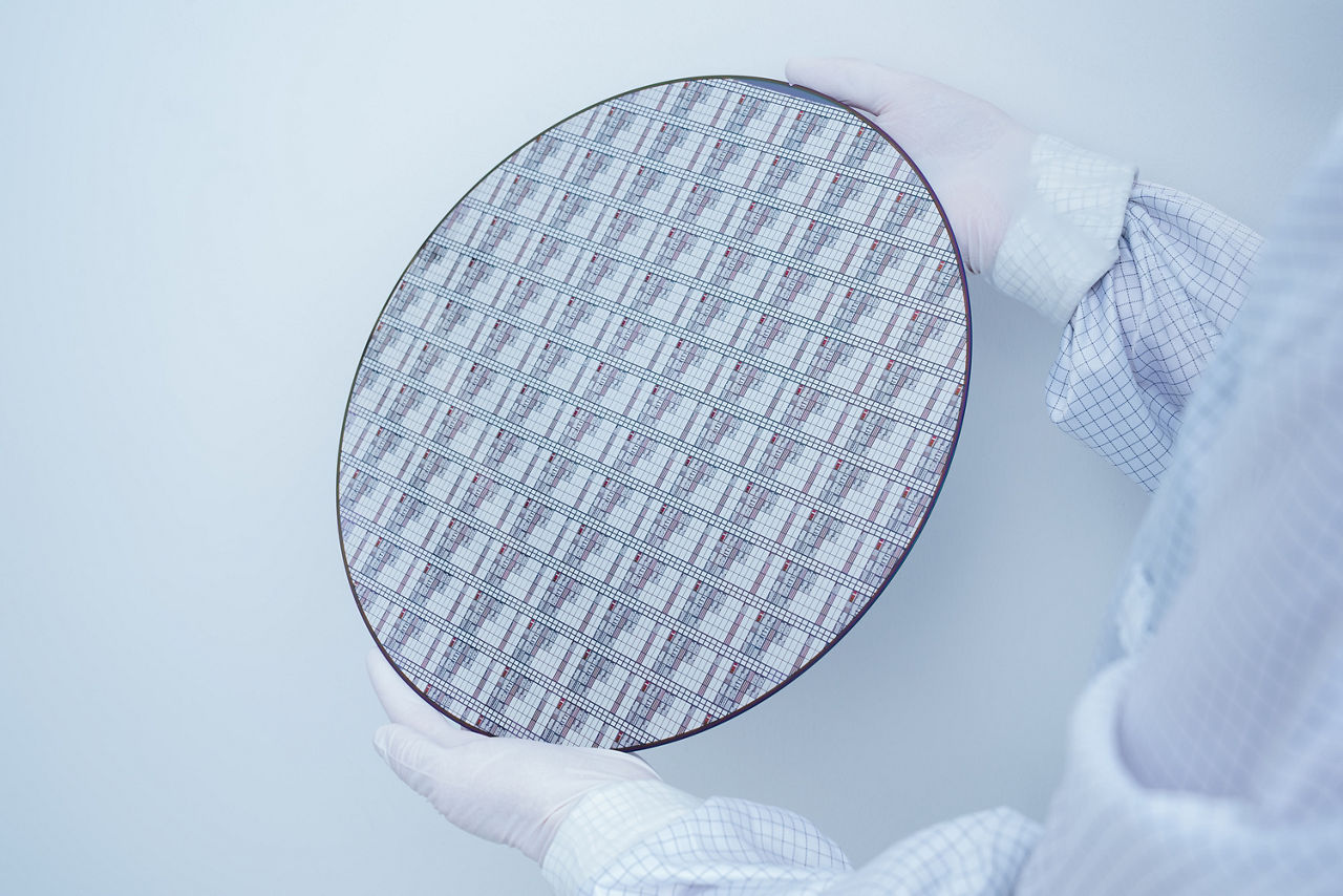
An LLC resonant converter is a highly efficient isolated DC-DC converter topology that changes one DC voltage to another by using a specialized resonant tank circuit. It is uniquely capable of "soft-switching," which means its transistors turn on and off when the voltage or current across them is near zero, eliminating the bulk of energy losses.
Here is how it works and how it differs from traditional alternatives:
The name LLC comes from the three specific reactive components that form its resonant tank:
- L (First L): A series resonant inductor (Lr).
- L (Second L): A parallel magnetizing inductor (Lm) built into the transformer.
- C: A series resonant capacitor (Cr).
These components act like a high-frequency filter. By changing the switching frequency of the incoming square-wave voltage, the converter alters the impedance of the tank, thereby regulating the output voltage.
To understand what makes the LLC converter unique, it helps to compare it to the two most common alternative topologies: Hard-Switched Converters (like standard Buck or Full-Bridge) and Phase-Shifted Full-Bridge (PSFB) converters.
- Switching Mechanism: Hard-switched converters force transistors to turn on and off while subjected to high currents and voltages simultaneously, creating massive heat and energy spikes. The LLC uses Zero Voltage Switching (ZVS) on the primary side, allowing the transistors to switch only when the voltage across them is already at zero.
- Frequency Limits: Because hard-switching losses scale linearly with frequency, traditional converters are limited to sub-100 kHz operation to prevent overheating. LLC converters easily scale into hundreds of kHz or even multi-megahertz regions, shrinking the physical size of transformers and capacitors.
- Soft-Switching Range: PSFBs can achieve ZVS, but usually only under heavy or full load conditions; at light loads, they lose this ability and drop in efficiency. The LLC resonant tank maintains ZVS over a much wider load range, from completely empty to full capacity.
- Secondary Diodes: PSFBs suffer from high voltage stress and reverse-recovery energy losses on the secondary-side output rectifiers. The LLC converter inherently achieves Zero Current Switching (ZCS) on the secondary side, turning off output diodes or transistors gently as the current naturally drops to zero, removing reverse-recovery spikes.
- Control Method: PSFBs regulate voltage by changing the phase overlap (duty cycle) of the transistors at a constant frequency. LLC converters keep a fixed 50% duty cycle but dynamically vary the operating frequency to steer up or down the resonant curve.
The name LLC comes from the three specific reactive components that form its resonant tank:
- L (First L): A series resonant inductor (Lr).
- L (Second L): A parallel magnetizing inductor (Lm) built into the transformer.
- C: A series resonant capacitor (Cr).
These components act like a high-frequency filter. By changing the switching frequency of the incoming square-wave voltage, the converter alters the impedance of the tank, thereby regulating the output voltage.
To understand what makes the LLC converter unique, it helps to compare it to the two most common alternative topologies: Hard-Switched Converters (like standard Buck or Full-Bridge) and Phase-Shifted Full-Bridge (PSFB) converters.
- Switching Mechanism: Hard-switched converters force transistors to turn on and off while subjected to high currents and voltages simultaneously, creating massive heat and energy spikes. The LLC uses Zero Voltage Switching (ZVS) on the primary side, allowing the transistors to switch only when the voltage across them is already at zero.
- Frequency Limits: Because hard-switching losses scale linearly with frequency, traditional converters are limited to sub-100 kHz operation to prevent overheating. LLC converters easily scale into hundreds of kHz or even multi-megahertz regions, shrinking the physical size of transformers and capacitors.
- Soft-Switching Range: PSFBs can achieve ZVS, but usually only under heavy or full load conditions; at light loads, they lose this ability and drop in efficiency. The LLC resonant tank maintains ZVS over a much wider load range, from completely empty to full capacity.
- Secondary Diodes: PSFBs suffer from high voltage stress and reverse-recovery energy losses on the secondary-side output rectifiers. The LLC converter inherently achieves Zero Current Switching (ZCS) on the secondary side, turning off output diodes or transistors gently as the current naturally drops to zero, removing reverse-recovery spikes.
- Control Method: PSFBs regulate voltage by changing the phase overlap (duty cycle) of the transistors at a constant frequency. LLC converters keep a fixed 50% duty cycle but dynamically vary the operating frequency to steer up or down the resonant curve.
Modern power electronics demand higher power density, lower thermal profiles, and unprecedented efficiency. Traditional isolated DC-DC conversion architectures struggle to meet these strict requirements due to inherent switching losses and material limitations of silicon (Si) MOSFET switch technology.
The integration of Gallium Nitride (GaN) High-Electron-Mobility Transistors (HEMTs) into LLC resonant converter topologies provides a solution to this problem. The LLC converter inherently enables Zero Voltage Switching (ZVS) across a wide operating range, minimizing turn-on losses. By replacing silicon MOSFETs with GaN devices, engineers can reduce parasitic capacitances, eliminate reverse recovery losses, and dramatically increase switching frequencies.
Power conversion design has entered an era defined by aggressive space constraints and stringent efficiency regulations. Industry standards such as 80 PLUS Titanium and Ruby for data center power supplies require over 96% peak efficiency, while electric vehicle (EV) onboard chargers must minimize weight and volume to maximize driving range.
Historically, hard-switched topologies like the phase-shifted full-bridge or interleaved buck-boost served as industry workhorses. However, these topologies suffer from significant switching losses that scale linearly with frequency. This restricts the operational frequency of silicon-based designs to under 100 kHz in most high-power applications, requiring large, heavy magnetic components and capacitors.
Soft-switching topologies, specifically the LLC resonant converter, overcome these operational frequency barriers. When combined with Gallium Nitride (GaN), the LLC resonant converter can operate efficiently in to the multi-megahertz range. This combination delivers a significant leap in power density and thermal management efficiency.
The LLC resonant converter is a member of the resonant tank DC-DC converter family. It is named for its three reactive tank components: a resonant capacitor (Cr), a series resonant inductor (Lr), and a parallel magnetizing inductor (Lm) typically integrated into the isolation transformer.
A standard isolated LLC resonant converter consists of four distinct operational blocks:
- Square generator: A half-bridge or full-bridge (shown above) configuration — the latter often built as a GaN full-bridge converter in higher-power designs — that converts the DC input voltage into a high-frequency square wave.
- Resonant Tank: Filters the high-frequency harmonics, presenting a sinusoidal current to the transformer primary based on the switching frequency.
- Transformer: Provides galvanic isolation and steps the voltage up or down.
- Rectifier: Converts alternating current (AC) into direct current (DC).
- Filter: A capacitive filter that smoothes the rectified AC current into a stable DC output voltage.
Silicon power MOSFETs have approached the physical limits dictated by their material properties. As a wide bandgap semiconductor, Gallium Nitride (GaN) provides superior material characteristics that fundamentally alter soft-switching circuit design.
A standard isolated LLC resonant converter consists of four distinct operational blocks:
- Square generator: A half-bridge or full-bridge (shown above) configuration — the latter often built as a GaN full-bridge converter in higher-power designs — that converts the DC input voltage into a high-frequency square wave.
- Resonant Tank: Filters the high-frequency harmonics, presenting a sinusoidal current to the transformer primary based on the switching frequency.
- Transformer: Provides galvanic isolation and steps the voltage up or down.
- Rectifier: Converts alternating current (AC) into direct current (DC).
- Filter: A capacitive filter that smoothes the rectified AC current into a stable DC output voltage.
Silicon power MOSFETs have approached the physical limits dictated by their material properties. As a wide bandgap semiconductor, Gallium Nitride (GaN) provides superior material characteristics that fundamentally alter soft-switching circuit design.
When comparing identical LLC converter topologies designed with Silicon versus GaN, the differences in parasitic parameters directly influence key design considerations such as overall efficiency, driving dynamics, and maximum operating frequency.
The output capacitance (Coss) of a switch dictates the amount of energy stored in the device during its off-state (Eoss = 1/2 x Coss x Vin²). In an LLC converter, even though ZVS eliminates turn-on losses, Qoss still impacts performance:
- Dead-Time Requirements: To achieve ZVS, the magnetizing current must fully discharge Qoss. Silicon devices have a high Qoss, requiring either a long dead-time or a high magnetizing current (low Lm). Long dead-times limit the maximum switching frequency and reduce the effective duty cycle, while low Lm values increase circulating currents and conduction losses.
- The GaN Advantage: GaN transistors can provide a substantial reduction in Qoss — often in the range of 70–90%, depending on the specific silicon device used for comparison — for an equivalent RDS(on). This allows designers to shorten dead-times from several hundred nanoseconds down to tens of nanoseconds. Additionally, they can specify a much higher Lm, reducing circulating current losses in the resonant tank.
When a silicon MOSFET body diode conducts during the dead-time window or under synchronous rectification, it stores a minority carrier charge (Qrr). If the switch is hard-commutated or subjected to a rapid voltage transient (dv/dt), this charge must be cleared. This creates a large reverse current spike, leading to high power dissipation, voltage ringing, and electromagnetic interference (EMI).
GaN transistors have a near-zero (negligible) Qrr. Because they lack a physical p-n junction, reverse conduction relies entirely on majority carriers in the 2DEG channel. This removes reverse recovery losses, protects the system from dv/dt-induced failures, and simplifies synchronous rectification timing control on the secondary side.
The gate charge (Qg) represents the total charge required to fully turn on the switch channel. Silicon MOSFETs feature high gate charges, requiring significant drive current from the gate driver circuit (Pgate = Qg x Vgate x fs).
GaN transistors exhibit extremely small gate charges, typically several times lower than comparable Silicon equivalents, depending on the specific parts compared. This drastically lowers gate drive power consumption, permitting multi-megahertz operation without overheating the gate drive integrated circuit (IC). It also allows for extremely fast gate turn-on and turn-off transitions.
The output capacitance (Coss) of a switch dictates the amount of energy stored in the device during its off-state (Eoss = 1/2 x Coss x Vin²). In an LLC converter, even though ZVS eliminates turn-on losses, Qoss still impacts performance:
- Dead-Time Requirements: To achieve ZVS, the magnetizing current must fully discharge Qoss. Silicon devices have a high Qoss, requiring either a long dead-time or a high magnetizing current (low Lm). Long dead-times limit the maximum switching frequency and reduce the effective duty cycle, while low Lm values increase circulating currents and conduction losses.
- The GaN Advantage: GaN transistors can provide a substantial reduction in Qoss — often in the range of 70–90%, depending on the specific silicon device used for comparison — for an equivalent RDS(on). This allows designers to shorten dead-times from several hundred nanoseconds down to tens of nanoseconds. Additionally, they can specify a much higher Lm, reducing circulating current losses in the resonant tank.
When a silicon MOSFET body diode conducts during the dead-time window or under synchronous rectification, it stores a minority carrier charge (Qrr). If the switch is hard-commutated or subjected to a rapid voltage transient (dv/dt), this charge must be cleared. This creates a large reverse current spike, leading to high power dissipation, voltage ringing, and electromagnetic interference (EMI).
GaN transistors have a near-zero (negligible) Qrr. Because they lack a physical p-n junction, reverse conduction relies entirely on majority carriers in the 2DEG channel. This removes reverse recovery losses, protects the system from dv/dt-induced failures, and simplifies synchronous rectification timing control on the secondary side.
The gate charge (Qg) represents the total charge required to fully turn on the switch channel. Silicon MOSFETs feature high gate charges, requiring significant drive current from the gate driver circuit (Pgate = Qg x Vgate x fs).
GaN transistors exhibit extremely small gate charges, typically several times lower than comparable Silicon equivalents, depending on the specific parts compared. This drastically lowers gate drive power consumption, permitting multi-megahertz operation without overheating the gate drive integrated circuit (IC). It also allows for extremely fast gate turn-on and turn-off transitions.
Using GaN in an LLC converter provides system-level advantages that extend beyond individual component efficiency.
Because GaN devices can switch cleanly in the megahertz range with minimal penalty, the physical size of the passive elements can be scaled down aggressively. The volume of both the resonant inductor (Lr) and resonant capacitor (Cr) decreases inversely with frequency.
Furthermore, transformer core volume shrinks at higher frequencies, enabling planar transformer configurations integrated directly into the multi-layer application PCB. This can compress the overall power supply volume by 50% to 70%, pushing power densities beyond 100 W/in³.
GaN-based LLC converters exhibit flat efficiency curves. At light loads, traditional converters suffer from disproportionately high fixed switching and gate drive losses. GaN's low gate charge and reduced Eoss minimize these fixed losses, keeping light-load efficiency high. At heavy loads, the reduction in circulating currents (enabled by a larger Lm) keeps conduction losses (I²R) in check.
Lower overall power dissipation means less heat needs to be rejected from the system. Heatsinks can be reduced in size or eliminated entirely, relying instead on surface-mount thermal vias within the PCB. Operating at lower internal junction temperatures also reduces thermal stress on surrounding components, extending the mean time between failures (MTBF) of the power supply unit.
Because GaN devices can switch cleanly in the megahertz range with minimal penalty, the physical size of the passive elements can be scaled down aggressively. The volume of both the resonant inductor (Lr) and resonant capacitor (Cr) decreases inversely with frequency.
Furthermore, transformer core volume shrinks at higher frequencies, enabling planar transformer configurations integrated directly into the multi-layer application PCB. This can compress the overall power supply volume by 50% to 70%, pushing power densities beyond 100 W/in³.
GaN-based LLC converters exhibit flat efficiency curves. At light loads, traditional converters suffer from disproportionately high fixed switching and gate drive losses. GaN's low gate charge and reduced Eoss minimize these fixed losses, keeping light-load efficiency high. At heavy loads, the reduction in circulating currents (enabled by a larger Lm) keeps conduction losses (I²R) in check.
Lower overall power dissipation means less heat needs to be rejected from the system. Heatsinks can be reduced in size or eliminated entirely, relying instead on surface-mount thermal vias within the PCB. Operating at lower internal junction temperatures also reduces thermal stress on surrounding components, extending the mean time between failures (MTBF) of the power supply unit.
The combination of GaN switching performance and LLC soft-switching dynamics is ideal for applications requiring high efficiency, compact size, and low weight.
Hyperscale data centers and high-power AI server clusters require highly efficient power infrastructure to minimize operating expenses and cooling requirements. The industry open standard (e.g., Open Compute Project OCP ORV3) dictates a transition toward a 48V DC power distribution architecture.
GaN LLC resonant converters are widely used to step down 400V DC input from the primary power factor correction (PFC) stage to a regulated 48V or 12V intermediate bus. This architecture delivers the 97%+ efficiency needed to achieve 80 PLUS Titanium and Ruby compliance.
Onboard chargers must convert residential or commercial AC grid power to charge the high-voltage traction battery pack (typically 400V or 800V). Space inside vehicles is limited, and every kilogram added directly reduces the vehicle's driving range.
For designs not implementing a single-stage topology with GaN bidirectional switches (BDS), a high-frequency GaN LLC converter reduces the size of the isolation transformer and EMI filter components. This helps downsize the OBC housing, lowering vehicle weight while ensuring efficient thermal dissipation to the vehicle's liquid cooling loop.
Telecom base stations and other communications equipment require isolated DC-DC bricks capable of converting high-voltage distribution lines down to standard -48V DC telecom buses. These modules operate in harsh ambient outdoor environments where active fan cooling is prone to failure.
GaN LLC converters operate reliably under conduction-cooled configurations, using minimal potting material and space while tolerating high ambient operating thresholds.
From ultra-slim OLED televisions to high-wattage USB-PD 3.1 laptop chargers (140W–240W), consumers demand pocket-sized chargers. GaN LLC topologies enable these adapters to run at high frequencies (100–500 kHz), turning bulky power bricks into sleek, compact travel accessories.
Hyperscale data centers and high-power AI server clusters require highly efficient power infrastructure to minimize operating expenses and cooling requirements. The industry open standard (e.g., Open Compute Project OCP ORV3) dictates a transition toward a 48V DC power distribution architecture.
GaN LLC resonant converters are widely used to step down 400V DC input from the primary power factor correction (PFC) stage to a regulated 48V or 12V intermediate bus. This architecture delivers the 97%+ efficiency needed to achieve 80 PLUS Titanium and Ruby compliance.
Onboard chargers must convert residential or commercial AC grid power to charge the high-voltage traction battery pack (typically 400V or 800V). Space inside vehicles is limited, and every kilogram added directly reduces the vehicle's driving range.
For designs not implementing a single-stage topology with GaN bidirectional switches (BDS), a high-frequency GaN LLC converter reduces the size of the isolation transformer and EMI filter components. This helps downsize the OBC housing, lowering vehicle weight while ensuring efficient thermal dissipation to the vehicle's liquid cooling loop.
Telecom base stations and other communications equipment require isolated DC-DC bricks capable of converting high-voltage distribution lines down to standard -48V DC telecom buses. These modules operate in harsh ambient outdoor environments where active fan cooling is prone to failure.
GaN LLC converters operate reliably under conduction-cooled configurations, using minimal potting material and space while tolerating high ambient operating thresholds.
From ultra-slim OLED televisions to high-wattage USB-PD 3.1 laptop chargers (140W–240W), consumers demand pocket-sized chargers. GaN LLC topologies enable these adapters to run at high frequencies (100–500 kHz), turning bulky power bricks into sleek, compact travel accessories.
The GaN-driven LLC resonant converter represents a major evolution in isolated DC-DC power management and resonant converter design. By marrying the soft-switching characteristics of the LLC topology with the low parasitic charges and high electron mobility of Gallium Nitride transistors, engineers can bypass the traditional performance trade-offs dictated by Silicon MOSFET limitations.
The elimination of reverse recovery loss, combined with massive reductions in output charge (Qoss) and gate charge (Qg), enables reliable high-efficiency operation at switching frequencies multiple times higher than legacy designs resulting in system-level benefits such as downsized passive magnetics, reduced thermal footprints, and exceptional power densities — make this combination the preferred architecture for modern high-performance power supply design.
Share in WeChat
Scan the QR code with your WeChat App to share this page.
What is an LLC resonant converter?
It is a high-efficiency DC/DC converter topology that uses a resonant circuit made of two inductors and one capacitor to shape voltage and current, enabling soft switching.
What are the main components of an LLC converter?
It consists of primary-side power switches, a resonant tank, a high-frequency isolation transformer, output rectifier, and filter.
What is "soft switching"?
It is a switching technique where the transistor turns on or off when the voltage or current across it is zero, drastically reducing switching losses.
What is Zero-Voltage Switching (ZVS)?
ZVS occurs when the voltage across a switching device drops to zero before the device is turned on, eliminating switching losses.
What is Zero-Current Switching (ZCS)?
ZCS happens when the current through a switching device drops to zero before it turns off, preventing large current spikes and reducing electromagnetic interference (EMI).
Why is the LLC topology popular?
It maintains high efficiency over wide line and load variations and eliminates the need for bulky output inductors, shrinking board space.
What does the "L-L-C" stand for?
It stands for the two inductive elements (the resonant inductor (LR) and magnetizing inductor (LM)) and one capacitive element (resonant capacitor (CR)) in the resonant tank.
What is a resonant tank?
It is the energy-storing, wave-shaping portion of an LLC resonant converter located between the primary-side switching bridge and the isolation transformer.