
- ASIC
- Battery management ICs
- Clocks and timing solutions
- ESD and surge protection devices
- Automotive Ethernet
- Evaluation Boards
- High reliability
- Isolation
- Memories
- Microcontroller
- Power
- RF
- Security and smart card solutions
- Sensor technology
- Small signal transistors and diodes
- Transceivers
- Universal Serial Bus (USB)
- Wireless connectivity
- Search Tools
- Technology
- Packages
- Product Information
- Ordering
- Overview
- Automotive Ethernet PHY for in-vehicle networking
- Automotive Ethernet Switches for in-vehicle networking
- Overview
- Embedded flash IP solutions
- Flash+RAM MCP solutions
- F-RAM (Ferroelectric RAM)
- NOR flash
- nvSRAM (non-volatile SRAM)
- PSRAM – Pseudostatic RAM
- Radiation hardened and high-reliability memories
- SRAMs (Static Random Access Memory)
- Wafer and die memory solutions
- Overview
- AURIX™ TriCore™ MCUs
- PSOC™ MCUs
- TRAVEO™ T2G MCUs
- XMC™ MCUs
- Legacy MCUs
- MOTIX™ motor control SoCs/SIPs
- Overview
- AC-DC power conversion
- Automotive conventional powertrain ICs
- Class D audio amplifier ICs
- Contactless power and sensing ICs
- DC-DC converters
- Diodes and thyristors (Si/SiC)
- eFuses
- Gallium nitride (GaN)
- Gate Driver ICs
- IGBTs – Insulated gate bipolar transistors
- Intelligent power modules (IPM)
- JFETs
- LED driver ICs
- Motor drivers
- MOSFETs
- Power modules
- Power supply ICs
- Protection and monitoring ICs
- Silicon carbide (SiC)
- Smart power switches
- Solid state relays and isolators
- Wireless charging ICs
- Overview
- Antenna cross switches
- Antenna tuners
- Bias and control
- Coupler
- Driver amplifiers
- Rad hard microwave and RF
- Low noise amplifiers (LNAs)
- RF diode
- RF switches
- RF transistors
- Wireless control receiver
- Overview
- Calypso® products
- CIPURSE™ products
- Contactless memories
- OPTIGA™ embedded security solutions
- SECORA™ security solutions
- Security controllers
- Smart card modules
- Smart solutions for government ID
- Overview
- ToF 3D image sensors
- Current sensors
- Gas sensors
- Inductive position sensors
- MEMS microphones
- Pressure sensors
- Radar sensors
- Magnetic position sensors
- Magnetic speed sensors
- Capacitive sensors
- Temperature sensors
- Battery sensors
- Digital X-ray
- Computed tomography
- Sensor interface ASICs
- Overview
- Bipolar transistors
- Diodes
- Small signal/small power MOSFET
- Overview
- Automotive transceivers
- Control communication
- Powerline communications
- Overview
- USB 2.0 peripheral controllers
- USB 3.2 peripheral controllers
- USB hub controllers
- USB PD high-voltage microcontrollers
- USB-C AC-DC and DC-DC charging solutions
- USB-C charging port controllers
- USB-C Power Delivery controllers
- Overview
- AIROC™ Automotive wireless
- AIROC™ Bluetooth® and multiprotocol
- AIROC™ connected MCU
- AIROC™ Wi-Fi + Bluetooth® combos
- AIROC™ Ultra-Wide Band Solutions
- Overview
- Commercial off-the-shelf (COTs) memory portfolio
- Defense memory portfolio
- High-reliability power conversion and management
- Overview
- Rad hard microwave and RF
- Radiation hardened power
- Space memory portfolio
- Overview
- Parallel NOR flash
- SEMPER™ NOR flash family
- SEMPER™ X1 LPDDR flash
- Serial NOR flash
- Overview
-
32-bit TriCore™ AURIX™ – TC2x
- Overview
- AURIX™ family – TC21xL
- AURIX™ family – TC21xSC (wireless charging)
- AURIX™ family – TC22xL
- AURIX™ family – TC23xL
- AURIX™ family – TC23xLA (ADAS)
- AURIX™ family – TC23xLX
- AURIX™ family – TC264DA (ADAS)
- AURIX™ family – TC26xD
- AURIX™ family – TC27xT
- AURIX™ family – TC297TA (ADAS)
- AURIX™ family – TC29xT
- AURIX™ family – TC29xTT (ADAS)
- AURIX™ family – TC29xTX
- AURIX™ TC2x emulation devices
-
32-bit TriCore™ AURIX™ – TC3x
- Overview
- AURIX™ family - TC32xLP
- AURIX™ family – TC33xDA
- AURIX™ family - TC33xLP
- AURIX™ family – TC35xTA (ADAS)
- AURIX™ family – TC36xDP
- AURIX™ family – TC37xTP
- AURIX™ family – TC37xTX
- AURIX™ family – TC38xQP
- AURIX™ family – TC39xXA (ADAS)
- AURIX™ family - TC39xXX/XP
- AURIX™ family – TC3Ex
- AURIX™ TC37xTE (emulation devices)
- AURIX™ TC39xXE (emulation devices)
- 32-bit TriCore™ AURIX™ – TC4x
- Overview
- PSOC™ 4 HV Arm® Cortex®-M0+
- PSOC™ 5 LP Arm® Cortex®-M3
- PSOC™ 6 Arm® Cortex®-M4/M0+
- PSOC™ Multitouch Touchscreen Controller
- PSOC™ Control C3 Arm® Cortex®-M33
- PSOC™ Automotive 4: Arm® Cortex®-M0/M0+
- PSOC™ Edge Arm® Cortex® M55/M33
- PSOC™ Control C1 Arm® Cortex®-M0
- Overview
- 32-bit TRAVEO™ T2G Arm® Cortex® for body
- 32-bit TRAVEO™ T2G Arm® Cortex® for cluster
- Overview
- 32-bit XMC1000 industrial microcontroller Arm® Cortex®-M0
- 32-bit XMC4000 industrial microcontroller Arm® Cortex®-M4
- XMC5000 Industrial Microcontroller Arm® Cortex®-M4F
- 32-bit XMC7000 Industrial Microcontroller Arm® Cortex®-M7
- Overview
- Legacy 32-bit MCU
- Legacy 8-bit/16-bit microcontroller
- Other legacy MCUs
- 32-bit FM Arm® Cortex® Microcontroller
- Sensing controllers
- Overview
- AC-DC integrated power stage - CoolSET™
- AC-DC PWM and PFC controller
- Overview
- Bridge rectifiers & AC switches
- CoolSiC™ Schottky diodes
- Diode bare dies
- Silicon diodes
- Thyristor / Diode Power Modules
- Thyristor soft starter modules
- Thyristor/diode discs
- Overview
- GaN bidirectional switches
- GaN smart
- GaN transistors (GaN HEMTs)
- GaN with integrated driver
- GaN bare dies
- Overview
- Automotive gate driver ICs
- Gate Driver ICs for GaN HEMTs
- Gate Driver ICs for SiC MOSFETs
- Half-Bridge Gate Driver ICs
- High-Side Gate Driver ICs
- Isolated Gate Driver ICs
- Level-Shift Gate Driver ICs
- Low-Side Gate Driver ICs
- Three-Phase Gate Driver ICs
- Transformer Driver ICs
- Overview
- AC-DC LED driver ICs
- Ballast IC
- DC-DC LED driver IC
- LED dimming interface IC
- Linear LED driver IC
- LITIX™ - Automotive LED Driver IC
- NFC wireless configuration IC with PWM output
- VCSEL driver
- Overview
- BLDC motor drivers
- BDC motor drivers
- Stepper & servo motor drivers
- Motor drivers with MCU
- Bridge drivers with MOSFETs
- Gate Driver ICs
- Overview
- Automotive MOSFET: 30 V to 800 V
- Dual MOSFETs
- MOSFET (Si & SiC) Modules
- N-channel depletion mode MOSFET
- N-channel MOSFETs
- P-channel MOSFETs
-
Silicon carbide CoolSiC™ MOSFETs
- Overview
- Silicon Carbide MOSFET modules
- Silicon carbide MOSFET discretes
- Silicon carbide MOSFETs bare dies
- 400 V / 440 V Silicon Carbide MOSFETs
- 650 V Silicon Carbide MOSFETs
- 750 V Silicon Carbide MOSFETs
- 1200 V Silicon Carbide MOSFETs
- 2000 V Silicon Carbide MOSFETs
- 2300 V Silicon Carbide MOSFETs
- 3300 V Silicon Carbide MOSFETs
- 1700 V Silicon Carbide MOSFETs
- Silicon Carbide Bidirectional Switches
- Small signal/small power MOSFET
- Overview
- IGBT modules
- MOSFET (Si & SiC) Modules
- Intelligent power modules (IPM)
- Diodes and thyristors (Si/SiC)
- Automotive IGBT and CoolSiC™ MOSFET modules
- High density power modules
- Overview
- Automotive transceivers
- Linear voltage regulators
- Power management ICs (PMIC)
- Automotive switching regulators
- System Basis Chips (SBC)
- Overview
- High-side switches
- Low-side switches
- Multichannel SPI Switches & Controller
- Automotive eFuses
- Overview
- Radar sensors for automotive
- Radar sensors for IoT
- Overview
- EZ-USB™ CX3 MIPI CSI2 to USB 3.0 camera controller
- EZ-USB™ FX10 & FX5N USB 10Gbps peripheral controller
- EZ-USB™ FX20 USB 20 Gbps peripheral controller
- EZ-USB™ FX3 USB 5 Gbps peripheral controller
- EZ-USB™ FX3S USB 5 Gbps peripheral controller with storage interface
- EZ-USB™ FX5 USB 5 Gbps peripheral controller
- EZ-USB™ SD3 USB 5 Gbps storage controller
- EZ-USB™ SX3 FIFO to USB 5 Gbps peripheral controller
- Overview
- EZ-PD™ PMG1-B1 Battery Charge Controller with USB-C PD MCU
- EZ-PD™ PMG1-S0 high-voltage MCU with USB-C and PD
- EZ-PD™ PMG1-S1 high-voltage MCU with USB-C and PD
- EZ-PD™ PMG1-S2 high-voltage MCU with USB PD
- EZ-PD™ PMG1-S3 high-voltage MCU with USB-C & PD
- EZ-PD™ PMG1-B2 Battery Charge Controller with USB-C PD MCU
- Overview
- EZ-PD™ CCG3 USB type-C port controller PD
- EZ-PD™ CCG3PA USB-C and PD
- EZ-PD™ CCG3PA-NFET USB-C PD controller
- EZ-PD™ CCG7x consumer USB-C Power Delivery & DC-DC controller
- EZ-PD™ PAG1: power adapter generation 1
- EZ-PD™ PAG2: Power Adapter Generation 2
- EZ-PD™ PAG2-PD USB-C PD Controller
- Overview
- EZ-PD™ ACG1F one-port USB-C controller
- EZ-PD™ CCG2 USB Type-C port controller
- EZ-PD™ CCG3PA Automotive USB-C and Power Delivery controller
- EZ-PD™ CCG4 two-port USB-C and PD
- EZ-PD™ CCG5 dual-port and CCG5C single-port USB-C PD controllers
- EZ-PD™ CCG6 one-port USB-C & PD controller
- EZ-PD™ CCG6_CFP and EZ-PD™ CCG8_CFP Dual-Single-Port USB-C PD
- EZ-PD™ CCG6DF dual-port and CCG6SF single-port USB-C PD controllers
- EZ-PD™ CCG7D Automotive dual-port USB-C PD + DC-DC controller
- EZ-PD™ CCG7S Automotive single-port USB-C PD solution with a DC-DC controller + FETs
- EZ-PD™ CCG8 dual-single-port USB-C PD
- EZ-PD™ CMG1 USB-C EMCA controller
- EZ-PD™ CMG2 USB-C EMCA controller with EPR
Browse by core architecture
Browse by key technologies
Browse by design resources & partners
- LATEST IN
- Aerospace and defense
- AI and data center
- Automotive
- Communications
- Consumer electronics
- Industrial
- Security solutions
- Smart home and building
- Solutions
- Overview
- Defense applications
- Space applications
- Overview
- Data center power solutions
- Edge computing
- Machine Learning Edge AI
- Overview
- ADAS & autonomous driving
- Automotive body electronics
- Automotive LED lighting systems
- Automotive zonal architecture
- Chassis control & safety
- Electric vehicle drivetrain system
- EV thermal management system
- In-vehicle infotainment & HMI
- Light electric vehicle solutions
- Overview
- Satellite communications
- Telecommunications infrastructure
- Overview
- AR and smart glasses
- Complete system solutions for smart TVs
- Consumer Wearables
- Drones
- Home appliances
- Mobile device and smartphone solutions
- Photovoltaic
- Power adapters and chargers
- Semiconductor solutions for home entertainment applications
- Smart conference systems
- Overview
- Asset Tracking
- Battery energy storage (BESS)
- Battery formation and testing
- Digital health
- Electric forklifts
- EV charging
- High voltage solid-state power distribution
- Hydrogen electrolysis
- Industrial & Medical SMPS
- Industrial automation
- Industrial motor drives and controls
- Industrial robots
- LED lighting system design
- Light electric vehicle solutions
- Photovoltaic
- Power adapters and chargers
- Power tools
- Power transmission and distribution
- Robotics
- Traction
- Uninterruptible power supplies (UPS)
- Wind power
- Overview
- Access control and ticketing
- Device authentication and brand protection
- Embedded security for the Internet of Things (IoT)
- eSIM applications
- Government identification
- Mobile security
- Payment solutions
- Overview
- Domestic robots
- Heating ventilation and air conditioning (HVAC)
- Home and building automation
- PC accessories
- Semiconductor solutions for home entertainment applications
- Overview
- Battery management systems (BMS)
- Connectivity
- Human Machine Interface
- Machine Learning Edge AI
- Motor control
- Power conversion
- Security
- Sensor solutions
- System diagnostics and analytics
- Overview
- Data center power distribution
- FPGAs in datacenter applications
- Power system reliability modeling
-
Server rack power management
- Overview
- AI accelerator cards
- AMD CPU voltage regulator Ics
- Ampere CPU voltage regulator Ics
- Intel CPU voltage regulator Ics
- Intermediate Bus Converter (IBC)
- Network switches for AI data centers and server racks
- Server battery backup units (BBU)
- Server power path protection
- Server power supply units (PSU)
- SmartNIC cards
- Overview
- Automotive animated LED lighting system
- Automotive LED front single light functions
- Automotive LED rear single light functions
- Full LED headlight system - multi-channel LED driver
- LED driver solutions for electric two- and three-wheelers
- LED pixel light controller - supply & communication
- Static interior ambient LED light
- Overview
- Active suspension control
- Automotive braking solutions
- Automotive steering solutions
- Chassis domain control
- Overview
-
Automotive battery management system
- Overview
- Automotive battery cell monitoring & balancing
- Automotive battery control unit (BCU)
- Automotive battery isolated communication
- Automotive battery management system (BMS) - 12 V to 24 V
- Automotive battery management system (BMS) - 48 V
- Automotive battery management system (BMS) - high-voltage
- Automotive battery pack monitoring
- Automotive battery passport & event logging
- Automotive battery protection & disconnection
- Automotive current sensing & coulomb counting
- BMS (electric two- & three-wheelers)
- Auxiliary inverter
- Auxiliary inverter - high-voltage (commercial vehicles)
- DC-DC converter high-voltage
- DC-DC converter high-voltage (commercial vehicles)
- EV charging
- EV traction inverter
- FCEV powertrain solutions
- On-board charging (electric commercial vehicles)
- On-board charging (OBC)
- On-board charging (OBC) solutions for electric two- and three-wheelers
- Traction inverter (electric commercial vehicles)
- Traction inverter (electric two- & three-wheelers)
- Overview
- Audio amplifier solutions
- Complete system solutions for smart TVs
- Distribution audio amplifier unit solutions
- Home theater installation speaker system solutions
- Party speaker solutions
- PoE audio amplifier unit solutions
- Portable speaker solutions
- Powered active speaker systems
- Remote control
- Smart speaker designs
- Soundbar solutions
- Overview
- Disposable healthcare equipment
- Durable healthcare equipment
- Healthcare wearables
- Overview
- Data center power solutions
- Digital input/output (I/O) modules
- DIN rail power supply solutions
- Home and building automation
- Industrial HMI Monitors and Panels
- Industrial motor drives and controls
- Industrial PC
- Industrial robots
- Machine vision
- Mobile robots (AGV, AMR)
- Programmable logic controller (PLC)
- Solid-state circuit breaker (SSCB)
- Uninterruptible power supplies (UPS)
- Overview
- Automotive battery management system
- Industrial and consumer BMS
- Overview
- AC-DC power conversion
- DC-DC power conversion
- Overview
- Power supply health monitoring
- LATEST IN
- Digital documentation
- Boards & Kits
- Finder & selection tools
- Platforms
- Services
- Simulation & Modeling
- Software
- Tools
- Partners
- Infineon for Makers
- University Alliance Program
- Overview
- Bipolar Discs Finder
- Bipolar Module Finder
- Connected Secure Systems Finder
- Diode Rectifier Finder
- ESD Protection Finder
- Evaluation Board Finder
- Gate Driver Finder
- IGBT Discrete Finder
- IGBT Module Finder
- IPM Finder
- Microcontroller Finder
- MOSFET Finder
- PMIC Finder
- PSOC™ and FMx MCU Board & Kit Finder
- Radar Finder
- Reference Design Finder
- Simulation Model Finder
- Smart Power Switch Finder
- Transceiver Finder
- Voltage Regulator Finder
- Wireless Connectivity Board & Kit Finder
- Infineon Gate Driver Recommendation Tool
- Overview
- AIROC™ software & tools
- AURIX™ software & tools
- DRIVECORE™ for automotive software development
- iMOTION™ software & tools
- Infineon Smart Power Switches & Gate Driver Tool Suite
- MOTIX™ software & tools
- OPTIGA™ software & tools
- PSOC™ software & tools
- TRAVEO™ software & tools
- XENSIV™ software & tools
- XMC™ software & tools
- Overview
- HiRel Fit Rate Tool
- Infineon Designer
- Interactive product sheet
- IPOSIM Online Power Simulation Platform
- InfineonSpice Offline Simulation Tool
- OPTIREG™ automotive power supply ICs Simulation Tool (PLECS)
- Power MOSFET Simulation Models
- PowerEsim Switch Mode Power Supply Design Tool
- Solution Finder
- XENSIV™ Magnetic Sensor Simulation Tool
- Overview
- Configuration
- Hardware Development
- Programming & Testing
- SDK
- Tools Archive
- Utilities
- Overview
- AURIX™ certifications
- AURIX™ development tools
-
AURIX™ Embedded Software
- Overview
- AURIX™ Applications software
- AURIX™ Artificial Intelligence
- AURIX™ Gateway
- AURIX™ iLLD Drivers
- Infineon safety
- AURIX™ Security
- AURIX™ TC3xx Motor Control Application Kit
- AURIX™ TC4x SW application architecture
- Infineon AUTOSAR
- Communication and Connectivity
- Middleware
- Non AUTOSAR OS/RTOS
- OTA
- AURIX™ Microcontroller Kits
- Overview
- TRAVEO™ Development Tools
- TRAVEO™ Embedded Software
- Overview
- XENSIV™ Development Tools
- XENSIV™ Embedded Software
- XENSIV™ evaluation boards
- Overview
- CAPSENSE™ Controllers Code Examples
- Memories for Embedded Systems Code Examples
- PSOC™ 1 Code Examples for PSOC™ Designer
- PSOC™ 3 Code Examples for PSOC™ Creator
- PSOC™ 3/4/5 Code Examples
- PSOC™ 4 Code Examples for PSOC™ Creator
- PSOC™ 6 Code Examples for PSOC™ Creator
- PSOC™ 63 Code Examples
- USB Controllers Code Examples
- Overview
- AIROC™ Wi-Fi & Bluetooth EZ-Serial Module Firmware Platform
- AIROC™ Wi-Fi & Bluetooth Linux and Android Drivers
- emWin Graphics Library and GUI for PSOC™
- Infineon Complex Device Driver for Battery Management Systems
- Memory Solutions Hub
- PSOC™ 6 Peripheral Driver Library (PDL) for PSOC™ Creator
- USB Controllers EZ-USB™ GX3 Software and Drivers
- Overview
- CAPSENSE™ Controllers Configuration Tools EZ-Click
- DC-DC Integrated POL Voltage Regulators Configuration Tool – PowIRCenter
- EZ-USB™ SX3 Configuration Utility
- FM+ Configuration Tools
- FMx Configuration Tools
- Tranceiver IC Configuration Tool
- USB EZ-PD™ Configuration Utility
- USB EZ-PD™ Dock Configuration Utility
- USB EZ-USB™ HX3C Blaster Plus Configuration Utility
- USB UART Config Utility
- XENSIV™ Tire Pressure Sensor Programming
- Overview
- EZ-PD™ CCGx Dock Software Development Kit
-
FMx Softune IDE
- Overview
- RealOS™ Real-Time Operating System
- Softune IDE Language tools
- Softune Workbench
- Tool Lineup for F2MC-16 Family SOFTUNE V3
- Tool Lineup for F2MC-8FX Family SOFTUNE V3
- Tool Lineup for FR Family SOFTUNE V6
- Virtual Starter Kit
- Windows 10 operation of released SOFTUNE product
- Windows 7 operation of released SOFTUNE product
- Windows 8 operation of released SOFTUNE product
- Infineon GUI Designer
- ModusToolbox™ Software
- PSOC™ Creator Software
- Radar Development Kit
- RUST
- USB Controllers SDK
- Wireless Connectivity Bluetooth Mesh Helper Applications
- XMC™ DAVE™ Software
- Overview
- AIROC™ Bluetooth® Connect App Archive
- Cypress™ Programmer Archive
- EZ-PD™ CCGx Power Software Development Kit Archive
- ModusToolbox™ Software Archive
- PSOC™ Creator Archive
- PSOC™ Designer Archive
- PSOC™ Programmer Archive
- USB EZ-PD™ Configuration Utility Archives
- USB EZ-PD™ Host SDK Archives
- USB EZ-USB™ FX3 Archive
- USB EZ-USB™ HX3PD Configuration Utility Archive
- WICED™ Smart SDK Archive
- WICED™ Studio Archive
- Overview
- Infineon Developer Center Launcher
- Infineon Register Viewer
- Pin and Code Wizard
- Timing Solutions
- Wireless Connectivity
- LATEST IN
- Support
- Training
- Developer Community
- News
Business & Financial Press
Oct 01, 2026
Business & Financial Press
Sep 29, 2026
Business & Financial Press
Sep 23, 2026
Business & Financial Press
Sep 16, 2026
- Company
- Our stories
- Events
- Press
- Investor
- Careers
- Quality
- Latest news
Business & Financial Press
Oct 01, 2026
Business & Financial Press
Sep 29, 2026
Business & Financial Press
Sep 23, 2026
Business & Financial Press
Sep 16, 2026
Why choose Infineon SiC modules?
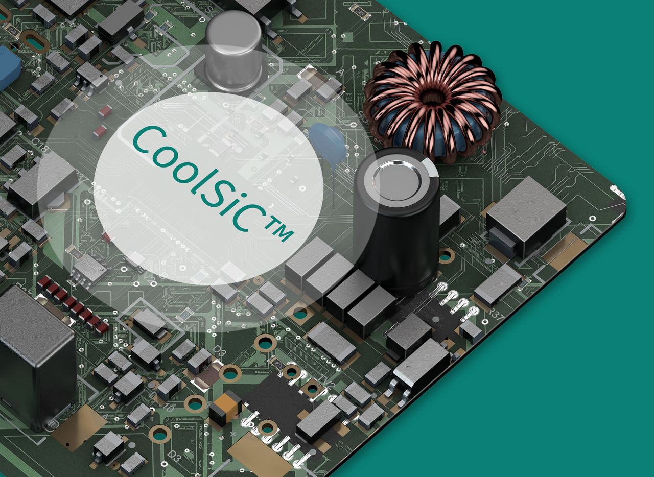
Infineon’s silicon carbide (SiC) modules help engineers increase efficiency, power density, and reliability in high-power applications. This value comes from a combination of CoolSiC™ technology, advanced packaging, .XT interconnection technology, proven reliability, large-scale manufacturing, supply-chain resilience, and decades of experience in SiC applications.
These advantages are especially valuable in DC EV charging, photovoltaic (PV), energy storage (ESS), uninterruptible power supplies (UPS), and traction applications, where reducing losses, increasing power density, and improving thermal performance are key priorities.
An online double-conversion UPS continuously processes power through an AC-DC rectifier and a DC-AC inverter, delivering a stable and clean AC output to critical loads regardless of input power disturbances. Many systems also include a bidirectional DC-DC converter that manages energy flow between the battery storage system and the DC link.
SiC power modules can be implemented in all major power-conversion stages, including the active front end (AFE), inverter, and bidirectional battery converter. By enabling higher efficiency and power density, SiC helps optimize UPS performance while reducing energy losses and thermal management requirements.
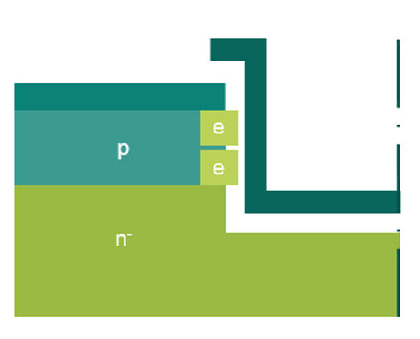
Trench-based SiC MOSFET architecture
Lower RDS(on) helps reduce conduction losses, while higher thermal headroom gives designers more options for increasing output power, reducing cooling effort, or improving margin.
Source: Infineon - Silicon carbide power modules in new EasyPACK™ C package enhance efficiency and lifetime of industrial applications.
In a nutshell, Infineon continuously builds on its experience in SiC technology to advance the performance, robustness, and system value of each CoolSiC™ generation. CoolSiC™ MOSFET M2 continues this innovation path with further developments in chip technology, packaging, and interconnection.
Power modules fail or age not only because of semiconductor behavior, but also because repeated heating and cooling stresses the die attach, bond connections, substrate, and other package interfaces.
In modules, Infineon’s .XT technology combines a highly reliable sintered die attach with copper front-side bond interconnection, improving thermal performance and power-cycling capability.
While .XT in discrete devices is based on diffusion-solder technology between the chip and lead frame, in power modules it refers to this combination of sintering and copper interconnection. This is a key contributor to the technology’s lifetime and reliability expectations.
In power modules, .XT technology results in more than 20× power-cycling capability versus standard interconnection technology under specified conditions, including Tvj,max = 175°C, ΔTvj = 100 K, and tcyc ≤ 3 s.
Combined with .XT interconnection technology, CoolSiC™ M2 enables more than 30% higher power density, up to 20× longer lifetime, and around 25% lower RDS(on) compared with the previous generation.
The concept is simple: if the package can conduct heat efficiently and tolerate repeated thermal expansion better, the module can support demanding load cycles with less derating.
In addition, power-cycling performance exceeded 90,000 cycles under harsh stress conditions, with no end-of-life indicators observed in the interconnection layer.
We offer CoolSiC™ power modules across established and newer package platforms, allowing designers to select the appropriate power level, footprint, topology, and integration approach.
The established EasyPACK™ B series includes baseplate-less modules in different package sizes 1B to 4B and circuit topologies for scalable inverter and converter designs. PressFIT pin-rivet connections support PCB-based assembly, while the flexible package platform with different package sizes addresses applications such as solar inverters, energy storage systems, onboard chargers, DC-DC converters, and auxiliary drives.
CoolSiC™ modules in EasyPACK™ C series address and support applications including fast DC EV charging, megawatt charging, energy storage, solid-state transformer (SST), solid-state circuit breaker (SSCB), and AI data centers. The package uses high-current PressFIT pins with twice the current capacity of standard and supports continuous operation up to 175°C and overload switching up to 200°C.
EasyPACK™ S is designed for compact, high-power-density systems, with a 5.6 mm module height and an approximately 33 × 36 mm² footprint. The first modules integrate 800 V and 1200 V CoolSiC™ MOSFETs based on second generation M2 technology, standard interconnection, a DBC substrate and PressFIT pins.
XHP™ 2 platform brings CoolSiC™ technology to applications such as traction, renewable-energy generation, and industrial power conversion. The 3.3 kV CoolSiC™ XHP™ 2 module family was nominated for the 2024 Deutscher Zukunftspreis.
Infineon complements its CoolSiC™ modules with EiceDRIVER™ gate driver ICs and XMC™, PSOC™ Control, and AURIX™ microcontrollers. XENSIV™ sensors and power-management solutions further support gate control, sensing, protection, and digital control in complete power-conversion systems.
For customers, SiC module selection is also a supply decision.
Infineon’s SiC manufacturing experience extends from commercial products based on 2-inch wafer technology in 2001 to today’s high-volume production using wafer diameter of 150 mm (6") and 200 mm (8") substrates.
Infineon’s first phase of the Kulim, Malaysia SiC power fab opened in August 2024, marking a major step toward establishing one of the industry's largest and most competitive 200 mm SiC power semiconductor manufacturing facilities.
For wide-bandgap technologies, the Villach, Austria, and Kulim, Malaysia sites operate as a "One Virtual Fab," leveraging shared technologies and processes to support efficient production ramp-up and operational consistency.
Our Smart Power Fab in Dresden, Germany, complements this manufacturing footprint by expanding 300 mm production capacity for power semiconductors and analog/mixed-signal components.
We further strengthen SiC supply-chain resilience through multiple wafer supply agreements with Wolfspeed, TanKeBlue, SK Siltron CSS, and Resonac. These agreements cover 150 mm materials and support the industry’s transition to 200 mm (8-inch) wafer diameters.
SiC devices are not simply “faster silicon.”
Infineon’s SiC reliability whitepaper explains that SiC-based devices require a different approach to reliability testing compared with Si. We consider many factors, like material properties, electric fields, switching speed, gate-oxide behavior, humidity robustness, body diode behavior, cosmic-ray robustness, and power-cycling effects when choosing the best process for design and reliability testing.
This matters for engineers because the application risk is not only whether a module switches efficiently on day one; it is whether the chip, gate oxide, package, and interconnect remain stable over the mission profile.
At Infineon, we draw on more than 25 years of SiC reliability expertise, combining mission-profile-based analysis, extended qualification, and rigorous validation testing to help customers build reliable, long-lasting systems.
Infineon SiC modules help engineers design more efficient, compact, reliable, and supply-resilient power systems by combining CoolSiC™ technology, robust packaging, broad module options, and scalable manufacturing.
Ready to make your next power design more efficient and supply-resilient?
1. What applications are Infineon SiC modules used for?
2. What is .XT interconnection technology in Infineon SiC modules?
.XT is Infineon’s extended-lifetime interconnection approach, implemented differently by product type. In discrete devices, .XT uses diffusion soldering between the chip and lead frame. In power modules, .XT combines sintered die attach with copper front-side bond interconnection to improve thermal performance and power-cycling capability.
3. Why does 200 mm SiC manufacturing matter?
The 200 mm SiC roadmap supports higher manufacturing efficiency and supply security from capacity scaling; Infineon announced the first 200 mm SiC product rollout from Villach in Q1 2025 and a Kulim transition from 150 mm to 200 mm wafers.