- ASIC
- Battery management ICs
- Clocks and timing solutions
- ESD and surge protection devices
- Automotive Ethernet
- Evaluation Boards
- High reliability
- Isolation
- Memories
- Microcontroller
- Power
- RF
- Security and smart card solutions
- Sensor technology
- Small signal transistors and diodes
- Transceivers
- Universal Serial Bus (USB)
- Wireless connectivity
- Search Tools
- Technology
- Packages
- Product Information
- Ordering
- Overview
- Automotive Ethernet PHY for in-vehicle networking
- Automotive Ethernet Switches for in-vehicle networking
- Overview
- Embedded flash IP solutions
- Flash+RAM MCP solutions
- F-RAM (Ferroelectric RAM)
- NOR flash
- nvSRAM (non-volatile SRAM)
- PSRAM – Pseudostatic RAM
- Radiation hardened and high-reliability memories
- SRAM (static RAM)
- Wafer and die memory solutions
- Overview
- AURIX™ TriCore™ MCUs
- PSOC™ MCUs
- TRAVEO™ T2G MCUs
- XMC™ MCUs
- Legacy MCUs
- MOTIX™ motor control SoCs/SIPs
- Overview
- AC-DC power conversion
- Automotive conventional powertrain ICs
- Class D audio amplifier ICs
- Contactless power and sensing ICs
- DC-DC converters
- Diodes and thyristors (Si/SiC)
- eFuses
- Gallium nitride (GaN)
- Gate Driver ICs
- IGBTs – Insulated gate bipolar transistors
- Intelligent power modules (IPM)
- JFETs
- LED driver ICs
- Motor drivers
- MOSFETs
- Power modules
- Power supply ICs
- Protection and monitoring ICs
- Silicon carbide (SiC)
- Smart power switches
- Solid state relays and isolators
- Wireless charging ICs
- Overview
- Antenna cross switches
- Antenna tuners
- Bias and control
- Coupler
- Driver amplifiers
- Rad hard microwave and RF
- Low noise amplifiers (LNAs)
- RF diode
- RF switches
- RF transistors
- Wireless control receiver
- Overview
- Calypso® products
- CIPURSE™ products
- Contactless memories
- OPTIGA™ embedded security solutions
- SECORA™ security solutions
- Security controllers
- Smart card modules
- Smart solutions for government ID
- Overview
- ToF 3D image sensors
- Current sensors
- Gas sensors
- Inductive position sensors
- MEMS microphones
- Pressure sensors
- Radar sensors
- Magnetic position sensors
- Magnetic speed sensors
- Capacitive sensors
- Temperature sensors
- Battery sensors
- Digital X-ray
- Computed tomography
- Sensor interface ASICs
- Overview
- Bipolar transistors
- Diodes
- Small signal/small power MOSFET
- Overview
- Automotive transceivers
- Control communication
- Powerline communications
- Overview
- USB 2.0 peripheral controllers
- USB 3.2 peripheral controllers
- USB hub controllers
- USB PD high-voltage microcontrollers
- USB-C AC-DC and DC-DC charging solutions
- USB-C charging port controllers
- USB-C Power Delivery controllers
- Overview
- AIROC™ Automotive wireless
- AIROC™ Bluetooth® and multiprotocol
- AIROC™ connected MCU
- AIROC™ Wi-Fi + Bluetooth® combos
- AIROC™ Ultra-Wide Band Solutions
- Overview
- Commercial off-the-shelf (COTs) memory portfolio
- Defense memory portfolio
- High-reliability power conversion and management
- Overview
- Rad hard microwave and RF
- Radiation hardened power
- Space memory portfolio
- Overview
- Parallel NOR flash
- SEMPER™ NOR flash family
- SEMPER™ X1 LPDDR flash
- Serial NOR flash
- Overview
-
32-bit TriCore™ AURIX™ – TC2x
- Overview
- AURIX™ family – TC21xL
- AURIX™ family – TC21xSC (wireless charging)
- AURIX™ family – TC22xL
- AURIX™ family – TC23xL
- AURIX™ family – TC23xLA (ADAS)
- AURIX™ family – TC23xLX
- AURIX™ family – TC264DA (ADAS)
- AURIX™ family – TC26xD
- AURIX™ family – TC27xT
- AURIX™ family – TC297TA (ADAS)
- AURIX™ family – TC29xT
- AURIX™ family – TC29xTT (ADAS)
- AURIX™ family – TC29xTX
- AURIX™ TC2x emulation devices
-
32-bit TriCore™ AURIX™ – TC3x
- Overview
- AURIX™ family - TC32xLP
- AURIX™ family – TC33xDA
- AURIX™ family - TC33xLP
- AURIX™ family – TC35xTA (ADAS)
- AURIX™ family – TC36xDP
- AURIX™ family – TC37xTP
- AURIX™ family – TC37xTX
- AURIX™ family – TC38xQP
- AURIX™ family – TC39xXA (ADAS)
- TC39xXX/XP
- AURIX™ family – TC3Ex
- AURIX™ TC37xTE (emulation devices)
- AURIX™ TC39xXE (emulation devices)
- 32-bit TriCore™ AURIX™ – TC4x
- Overview
- PSOC™ 4 Arm® Cortex®-M0/M0+
- PSOC™ 4 HV Arm® Cortex®-M0+
- PSOC™ 5 LP Arm® Cortex®-M3
- PSOC™ 6 Arm® Cortex®-M4/M0+
- PSOC™ Multitouch Touchscreen Controller
- PSOC™ Control C3 Arm® Cortex®-M33
- PSOC™ Automotive 4: Arm® Cortex®-M0/M0+
- PSOC™ Edge Arm® Cortex® M55/M33
- PSOC™ Control C1 Arm® Cortex®-M0
- Overview
- 32-bit TRAVEO™ T2G Arm® Cortex® for body
- 32-bit TRAVEO™ T2G Arm® Cortex® for cluster
- Overview
- 32-bit XMC1000 industrial microcontroller Arm® Cortex®-M0
- 32-bit XMC4000 industrial microcontroller Arm® Cortex®-M4
- XMC5000 Industrial Microcontroller Arm® Cortex®-M4F
- 32-bit XMC7000 Industrial Microcontroller Arm® Cortex®-M7
- Overview
- Legacy 32-bit MCU
- Legacy 8-bit/16-bit microcontroller
- Other legacy MCUs
- 32-bit FM Arm® Cortex® Microcontroller
- Sensing controllers
- Overview
- AC-DC integrated power stage - CoolSET™
- AC-DC PWM and PFC controller
- Overview
- Bridge rectifiers & AC switches
- CoolSiC™ Schottky diodes
- Diode bare dies
- Silicon diodes
- Thyristor / Diode Power Modules
- Thyristor soft starter modules
- Thyristor/diode discs
- Overview
- GaN bidirectional switches
- GaN smart
- GaN transistors (GaN HEMTs)
- GaN with integrated driver
- GaN bare dies
- Overview
- Automotive gate driver ICs
- Gate Driver ICs for GaN HEMTs
- Gate Driver ICs for SiC MOSFETs
- Half-Bridge Gate Driver ICs
- High-Side Gate Driver ICs
- Isolated Gate Driver ICs
- Level-Shift Gate Driver ICs
- Low-Side Gate Driver ICs
- Three-Phase Gate Driver ICs
- Transformer Driver ICs
- Overview
- AC-DC LED driver ICs
- Ballast IC
- DC-DC LED driver IC
- LED dimming interface IC
- Linear LED driver IC
- LITIX™ - Automotive LED Driver IC
- NFC wireless configuration IC with PWM output
- VCSEL driver
- Overview
- BLDC motor drivers
- BDC motor drivers
- Stepper & servo motor drivers
- Motor drivers with MCU
- Bridge drivers with MOSFETs
- Gate Driver ICs
- Overview
- Automotive MOSFET
- Dual MOSFETs
- MOSFET (Si & SiC) Modules
- N-channel depletion mode MOSFET
- N-channel MOSFETs
- P-channel MOSFETs
-
Silicon carbide CoolSiC™ MOSFETs
- Overview
- Silicon Carbide MOSFET modules
- Silicon carbide MOSFET discretes
- Silicon carbide MOSFETs bare dies
- 400 V / 440 V Silicon Carbide MOSFETs
- 650 V Silicon Carbide MOSFETs
- 750 V Silicon Carbide MOSFETs
- 1200 V Silicon Carbide MOSFETs
- 2000 V Silicon Carbide MOSFETs
- 2300 V Silicon Carbide MOSFETs
- 3300 V Silicon Carbide MOSFETs
- 1700 V Silicon Carbide MOSFETs
- Small signal/small power MOSFET
- Overview
- IGBT modules
- MOSFET (Si & SiC) Modules
- Intelligent power modules (IPM)
- Diodes and thyristors (Si/SiC)
- Automotive IGBT and CoolSiC™ MOSFET modules
- High density power modules
- Overview
- Automotive transceivers
- Linear voltage regulators for automotive applications
- OPTIREG™ PMIC
- OPTIREG™ switcher
- OPTIREG™ System Basis Chips (SBC)
- Overview
- High-side switches
- Low-side switches
- Multichannel SPI Switches & Controller
- Automotive eFuses
- Overview
- Radar sensors for automotive
- Radar sensors for IoT
- Overview
- EZ-USB™ CX3 MIPI CSI2 to USB 3.0 camera controller
- EZ-USB™ FX10 & FX5N USB 10Gbps peripheral controller
- EZ-USB™ FX20 USB 20 Gbps peripheral controller
- EZ-USB™ FX3 USB 5 Gbps peripheral controller
- EZ-USB™ FX3S USB 5 Gbps peripheral controller with storage interface
- EZ-USB™ FX5 USB 5 Gbps peripheral controller
- EZ-USB™ SD3 USB 5 Gbps storage controller
- EZ-USB™ SX3 FIFO to USB 5 Gbps peripheral controller
- Overview
- EZ-PD™ PMG1-B1 Battery Charge Controller with USB-C PD MCU
- EZ-PD™ PMG1-S0 high-voltage MCU with USB-C and PD
- EZ-PD™ PMG1-S1 high-voltage MCU with USB-C and PD
- EZ-PD™ PMG1-S2 high-voltage MCU with USB PD
- EZ-PD™ PMG1-S3 high-voltage MCU with USB-C & PD
- EZ-PD™ PMG1-B2 Battery Charge Controller with USB-C PD MCU
- Overview
- EZ-PD™ CCG3 USB type-C port controller PD
- EZ-PD™ CCG3PA USB-C and PD
- EZ-PD™ CCG3PA-NFET USB-C PD controller
- EZ-PD™ CCG7x consumer USB-C Power Delivery & DC-DC controller
- EZ-PD™ PAG1: power adapter generation 1
- EZ-PD™ PAG2: Power Adapter Generation 2
- EZ-PD™ PAG2-PD USB-C PD Controller
- Overview
- EZ-PD™ ACG1F one-port USB-C controller
- EZ-PD™ CCG2 USB Type-C port controller
- EZ-PD™ CCG3PA Automotive USB-C and Power Delivery controller
- EZ-PD™ CCG4 two-port USB-C and PD
- EZ-PD™ CCG5 dual-port and CCG5C single-port USB-C PD controllers
- EZ-PD™ CCG6 one-port USB-C & PD controller
- EZ-PD™ CCG6_CFP and EZ-PD™ CCG8_CFP Dual-Single-Port USB-C PD
- EZ-PD™ CCG6DF dual-port and CCG6SF single-port USB-C PD controllers
- EZ-PD™ CCG7D Automotive dual-port USB-C PD + DC-DC controller
- EZ-PD™ CCG7S Automotive single-port USB-C PD solution with a DC-DC controller + FETs
- EZ-PD™ CCG8 dual-single-port USB-C PD
- EZ-PD™ CMG1 USB-C EMCA controller
- EZ-PD™ CMG2 USB-C EMCA controller with EPR
Browse by core architecture
Browse by key technologies
- LATEST IN
- Aerospace and defense
- AI and data center
- Automotive
- Communications
- Consumer electronics
- Health and lifestyle
- Industrial
- Security solutions
- Smart home and building
- Solutions
- Overview
- Defense applications
- Space applications
- Overview
- Data center power solutions
- Edge computing
- Machine Learning Edge AI
- Overview
- ADAS & autonomous driving
- Automotive body electronics
- Automotive LED lighting systems
- Automotive zonal architecture
- Chassis control & safety
- Electric vehicle drivetrain system
- EV thermal management system
- In-vehicle infotainment & HMI
- Light electric vehicle solutions
- Overview
- Satellite communications
- Telecommunications infrastructure
- Overview
- Power adapters and chargers
- Complete system solutions for smart TVs
- Mobile device and smartphone solutions
- Semiconductor solutions for home entertainment applications
- Smart conference systems
- Drones
- AR and smart glasses
- Photovoltaic
- Consumer Wearables
- Home appliances
- Overview
- Power adapters and chargers
- Asset Tracking
- Battery formation and testing
- Electric forklifts
- Battery energy storage (BESS)
- EV charging
- High voltage solid-state power distribution
- Industrial automation
- Industrial motor drives and controls
- Industrial robots
- LED lighting system design
- Light electric vehicle solutions
- Power transmission and distribution
- Traction
- Uninterruptible power supplies (UPS)
- Digital health
- Robotics
- Wind power
- Hydrogen electrolysis
- Photovoltaic
- Industrial & Medical SMPS
- Power tools
- Overview
- Device authentication and brand protection
- Embedded security for the Internet of Things (IoT)
- eSIM applications
- Government identification
- Mobile security
- Payment solutions
- Access control and ticketing
- Overview
- Domestic robots
- Heating ventilation and air conditioning (HVAC)
- Home and building automation
- PC accessories
- Semiconductor solutions for home entertainment applications
- Overview
- Battery management systems (BMS)
- Connectivity
- Human Machine Interface
- Machine Learning Edge AI
- Motor control
- Power conversion
- Security
- Sensor solutions
- System diagnostics and analytics
- Overview
- FPGAs in datacenter applications
- Power system reliability modeling
-
Server rack power management
- Overview
- Server power supply units (PSU)
- Server battery backup units (BBU)
- Intermediate Bus Converter (IBC)
- Ampere CPU voltage regulator Ics
- Intel CPU voltage regulator Ics
- AMD CPU voltage regulator Ics
- AI accelerator cards
- SmartNIC cards
- Network switches for AI data centers and server racks
- Server power path protection
- Data center power distribution
- Overview
- Automotive animated LED lighting system
- Automotive LED front single light functions
- Automotive LED rear single light functions
- Full LED headlight system - multi-channel LED driver
- LED drivers (electric two- & three-wheelers)
- LED pixel light controller - supply & communication
- Static interior ambient LED light
- Overview
- Active suspension control
- Automotive braking solutions
- Automotive steering solutions
- Chassis domain control
- Overview
-
Automotive BMS
- Overview
- Automotive battery cell monitoring & balancing
- Automotive battery control unit (BCU)
- Automotive battery isolated communication
- Automotive battery management system (BMS) - 12 V to 24 V
- Automotive battery management system (BMS) - 48 V
- Automotive battery management system (BMS) - high-voltage
- Automotive battery pack monitoring
- Automotive battery passport & event logging
- Automotive battery protection & disconnection
- Automotive current sensing & coulomb counting
- BMS (electric two- & three-wheelers)
- EV charging
- FCEV powertrain system
- Auxiliary inverter
- Auxiliary inverter - high-voltage (commercial vehicles)
- EV traction inverter
- Traction inverter (electric commercial vehicles)
- Traction inverter (electric two- & three-wheelers)
- DC-DC converter high-voltage
- DC-DC converter high-voltage (commercial vehicles)
- On-board charging (electric commercial vehicles)
- On-board charging (OBC)
- On-board charging (OBC) solutions for electric two- and three-wheelers
- Overview
- AC-DC power conversion for telecommunications infrastructure
- DC-DC power conversion for telecommunications infrastructure
- FPGA in wired and wireless telecommunications applications
- Power system reliability modeling
- RF front end components for telecommunications infrastructure
- Memory solutions for cellular base stations
- Security solutions for cellular base stations
- Overview
- Audio amplifier solutions
- Complete system solutions for smart TVs
- Distribution audio amplifier unit solutions
- Home theater installation speaker system solutions
- Party speaker solutions
- PoE audio amplifier unit solutions
- Portable speaker solutions
- Powered active speaker systems
- Remote control
- Smart speaker designs
- Soundbar solutions
- Overview
- Data center power solutions
- Digital input/output (I/O) modules
- DIN rail power supply solutions
- Home and building automation
- Industrial HMI Monitors and Panels
- Industrial motor drives and controls
- Industrial PC
- Industrial robots
- Machine vision
- Mobile robots (AGV, AMR)
- Programmable logic controller (PLC)
- Solid-state circuit breaker (SSCB)
- Uninterruptible power supplies (UPS)
- Overview
- Durable healthcare equipment
- Disposable healthcare equipment
- Healthcare wearables
- Overview
- Automotive BMS
- Industrial and consumer BMS
- Overview
- AC-DC power conversion
- DC-DC power conversion
- Overview
- Power supply health monitoring
- LATEST IN
- Digital documentation
- Boards & Kits
- Finder & selection tools
- Platforms
- Services
- Simulation & Modeling
- Software
- Tools
- Partners
- Infineon for Makers
- University Alliance Program
- Overview
- Bipolar Discs Finder
- Bipolar Module Finder
- Connected Secure Systems Finder
- Diode Rectifier Finder
- ESD Protection Finder
- Evaluation Board Finder
- Gate Driver Finder
- IGBT Discrete Finder
- IGBT Module Finder
- IPM Finder
- Microcontroller Finder
- MOSFET Finder
- PMIC Finder
- Product Finder
- PSOC™ and FMx MCU Board & Kit Finder
- Radar Finder
- Reference Design Finder
- Simulation Model Finder
- Smart Power Switch Finder
- Transceiver Finder
- Voltage Regulator Finder
- Wireless Connectivity Board & Kit Finder
- Overview
- AIROC™ software & tools
- AURIX™ software & tools
- DRIVECORE™ for automotive software development
- iMOTION™ software & tools
- Infineon Smart Power Switches & Gate Driver Tool Suite
- MOTIX™ software & tools
- OPTIGA™ software & tools
- PSOC™ software & tools
- TRAVEO™ software & tools
- XENSIV™ software & tools
- XMC™ software & tools
- Overview
- CoolGaN™ Simulation Tool (PLECS)
- HiRel Fit Rate Tool
- Infineon Designer
- Interactive product sheet
- IPOSIM Online Power Simulation Platform
- InfineonSpice Offline Simulation Tool
- OPTIREG™ automotive power supply ICs Simulation Tool (PLECS)
- Power MOSFET Simulation Models
- PowerEsim Switch Mode Power Supply Design Tool
- Solution Finder
- XENSIV™ Magnetic Sensor Simulation Tool
- Overview
- AURIX™ certifications
- AURIX™ development tools
-
AURIX™ Embedded Software
- Overview
- AURIX™ Applications software
- AURIX™ Artificial Intelligence
- AURIX™ Gateway
- AURIX™ iLLD Drivers
- Infineon safety
- AURIX™ Security
- AURIX™ TC3xx Motor Control Application Kit
- AURIX™ TC4x SW application architecture
- Infineon AUTOSAR
- Communication and Connectivity
- Middleware
- Non AUTOSAR OS/RTOS
- OTA
- AURIX™ Microcontroller Kits
- Overview
- TRAVEO™ Development Tools
- TRAVEO™ Embedded Software
- Overview
- XENSIV™ Development Tools
- XENSIV™ Embedded Software
- XENSIV™ evaluation boards
- Overview
- CAPSENSE™ Controllers Code Examples
- Memories for Embedded Systems Code Examples
- PSOC™ 1 Code Examples for PSOC™ Designer
- PSOC™ 3 Code Examples for PSOC™ Creator
- PSOC™ 3/4/5 Code Examples
- PSOC™ 4 Code Examples for PSOC™ Creator
- PSOC™ 6 Code Examples for PSOC™ Creator
- PSOC™ 63 Code Examples
- USB Controllers Code Examples
- Overview
- DEEPCRAFT™ AI Hub
- DEEPCRAFT™ Audio Enhancement
- DEEPCRAFT™ Model Converter
-
DEEPCRAFT™ Ready Models
- Overview
- DEEPCRAFT™ Ready Model for Baby Cry Detection
- DEEPCRAFT™ Ready Model for Cough Detection
- DEEPCRAFT™ Ready Model for Direction of Arrival (Sound)
- DEEPCRAFT™ Ready Model for Factory Alarm Detection
- DEEPCRAFT™ Ready Model for Fall Detection
- DEEPCRAFT™ Ready Model for Gesture Classification
- DEEPCRAFT™ Ready Model for Siren Detection
- DEEPCRAFT™ Ready Model for Snore Detection
- DEEPCRAFT™ Studio
- DEEPCRAFT™ Voice Assistant
- Overview
- AIROC™ Wi-Fi & Bluetooth EZ-Serial Module Firmware Platform
- AIROC™ Wi-Fi & Bluetooth Linux and Android Drivers
- emWin Graphics Library and GUI for PSOC™
- Infineon Complex Device Driver for Battery Management Systems
- Memory Solutions Hub
- PSOC™ 6 Peripheral Driver Library (PDL) for PSOC™ Creator
- USB Controllers EZ-USB™ GX3 Software and Drivers
- Overview
- CAPSENSE™ Controllers Configuration Tools EZ-Click
- DC-DC Integrated POL Voltage Regulators Configuration Tool – PowIRCenter
- EZ-USB™ SX3 Configuration Utility
- FM+ Configuration Tools
- FMx Configuration Tools
- Tranceiver IC Configuration Tool
- USB EZ-PD™ Configuration Utility
- USB EZ-PD™ Dock Configuration Utility
- USB EZ-USB™ HX3C Blaster Plus Configuration Utility
- USB UART Config Utility
- XENSIV™ Tire Pressure Sensor Programming
- Overview
- EZ-PD™ CCGx Dock Software Development Kit
-
FMx Softune IDE
- Overview
- RealOS™ Real-Time Operating System
- Softune IDE Language tools
- Softune Workbench
- Tool Lineup for F2MC-16 Family SOFTUNE V3
- Tool Lineup for F2MC-8FX Family SOFTUNE V3
- Tool Lineup for FR Family SOFTUNE V6
- Virtual Starter Kit
- Windows 10 operation of released SOFTUNE product
- Windows 7 operation of released SOFTUNE product
- Windows 8 operation of released SOFTUNE product
- ModusToolbox™ Software
- PSOC™ Creator Software
- Radar Development Kit
- RUST
- USB Controllers SDK
- Wireless Connectivity Bluetooth Mesh Helper Applications
- XMC™ DAVE™ Software
- Overview
- AIROC™ Bluetooth® Connect App Archive
- Cypress™ Programmer Archive
- EZ-PD™ CCGx Power Software Development Kit Archive
- ModusToolbox™ Software Archive
- PSOC™ Creator Archive
- PSOC™ Designer Archive
- PSOC™ Programmer Archive
- USB EZ-PD™ Configuration Utility Archives
- USB EZ-PD™ Host SDK Archives
- USB EZ-USB™ FX3 Archive
- USB EZ-USB™ HX3PD Configuration Utility Archive
- WICED™ Smart SDK Archive
- WICED™ Studio Archive
- Overview
- Infineon Developer Center Launcher
- Infineon Register Viewer
- Pin and Code Wizard
- Timing Solutions
- Wireless Connectivity
- LATEST IN
- Support
- Training
- Developer Community
- News
Business & Financial Press
Jul 13, 2026
Business & Financial Press
Jul 07, 2026
Business & Financial Press
Jul 03, 2026
Business & Financial Press
Jul 02, 2026
- Company
- Our stories
- Events
- Press
- Investor
- Careers
- Quality
- Latest news
Business & Financial Press
Jul 13, 2026
Business & Financial Press
Jul 07, 2026
Business & Financial Press
Jul 03, 2026
Business & Financial Press
Jul 02, 2026
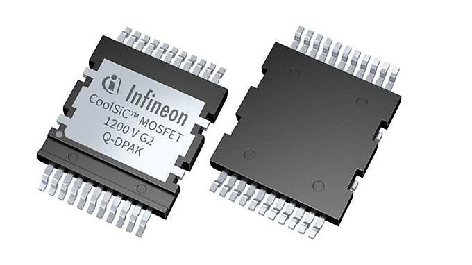
Infineon’s CoolSiC™ MOSFETs 1200 V G2 in a Q-DPAK package enable higher power density for industrial applications
Technology news
Munich, Germany – 29 July 2025 – Infineon Technologies AG (FSE: IFX / OTCQX: IFNNY) has launched the CoolSiC™ MOSFETs 1200 V G2 in a top-side-cooled (TSC) Q-DPAK package. The new devices deliver optimized thermal performance, system efficiency, and power density. They were specifically designed for demanding industrial applications that require high performance and reliability, such as electric vehicle chargers, solar inverters, uninterruptible power supplies, motor drives, and solid-state circuit breakers.
The new CoolSiC 1200 V G2 technology offers significant improvements over the previous generation, enabling up to 25 percent lower switching losses for equivalent RDS(on) devices, thereby increasing system efficiency by up to 0.1 percent. Utilizing Infineon's improved .XT die attach interconnection technology, the G2 devices achieve more than 15 percent lower thermal resistance and an 11 percent reduction in MOSFET temperature compared to G1 family products. The outstanding RDS(on) values, ranging from 4 mΩ to 78 mΩ, along with a broad product portfolio enable designers the flexibility to optimize system performance for their target applications. Furthermore, the new technology supports overload operation up to a junction temperature (Tvj) of 200°C and features high robustness against parasitic turn-on, ensuring reliable operation under dynamic and demanding conditions.
The CoolSiC MOSFETs 1200 V G2 are available in two Q-DPAK configurations: a single switch and a dual half-bridge. Both variants are part of Infineon’s broader X-DPAK top-side cooling platform. With a standardized package height of 2.3 mm across all TSC variants – including Q-DPAK and TOLT – the platform offers design flexibility and enables customers to scale and combine different products under a single heatsink assembly. This design flexibility simplifies advanced power system development, making it easier for customers to customize and scale their solutions.
The Q-DPAK package enhances thermal performance by enabling direct heat dissipation from the device’s top surface to the heatsink. This direct thermal path delivers significantly better heat transfer efficiency compared to traditional bottom-side cooled packages, enabling more compact designs. Additionally, the Q-DPAK package layout design allows for minimized parasitic inductance, which is critical for higher switching speeds. This enhances system efficiency and reduces voltage overshoot risk. The small footprint of the package supports compact system designs, while its compatibility with automated assembly processes simplifies manufacturing, ensuring cost-efficiency and scalability.
Availability
The CoolSiC MOSFET 1200 V G2 in Q-DPAK single switch and dual half-bridge package variants are available now. Further information is available at www.infineon.com/coolsic-mosfet-discretes.
Infineon Technologies AG is a global semiconductor leader in power systems and IoT. Infineon drives decarbonization and digitalization with its products and solutions. The Company had around 58,060 employees worldwide (end of September 2024) and generated revenue of about €15 billion in the 2024 fiscal year (ending 30 September). Infineon is listed on the Frankfurt Stock Exchange (ticker symbol: IFX) and in the USA on the OTCQX International over-the-counter market (ticker symbol: IFNNY).
Press Photos
The CoolSiC™ MOSFETs 1200 V G2 in a top-side-cooled Q-DPAK package enable higher power density for industrial applications
JPEG
2126x1535 px
Information Number : INFGIP202507-128

Veronika Seifried
Spokesperson Industrial and Infrastructure, GIP Division
+49 89 234 61662