- ASIC
- Battery management ICs
- Clocks and timing solutions
- ESD and surge protection devices
- Automotive Ethernet
- Evaluation Boards
- High reliability
- Isolation
- Memories
- Microcontroller
- Power
- RF
- Security and smart card solutions
- Sensor technology
- Small signal transistors and diodes
- Transceivers
- Universal Serial Bus (USB)
- Wireless connectivity
- Search Tools
- Technology
- Packages
- Product Information
- Ordering
- Overview
- Automotive Ethernet PHY for in-vehicle networking
- Automotive Ethernet Switches for in-vehicle networking
- Overview
- Embedded flash IP solutions
- Flash+RAM MCP solutions
- F-RAM (Ferroelectric RAM)
- NOR flash
- nvSRAM (non-volatile SRAM)
- PSRAM – Pseudostatic RAM
- Radiation hardened and high-reliability memories
- SRAM (static RAM)
- Wafer and die memory solutions
- Overview
- AURIX™ TriCore™ MCUs
- PSOC™ MCUs
- TRAVEO™ T2G MCUs
- XMC™ MCUs
- Legacy MCUs
- MOTIX™ motor control SoCs/SIPs
- Overview
- AC-DC power conversion
- Automotive conventional powertrain ICs
- Class D audio amplifier ICs
- Contactless power and sensing ICs
- DC-DC converters
- Diodes and thyristors (Si/SiC)
- eFuses
- Gallium nitride (GaN)
- Gate Driver ICs
- IGBTs – Insulated gate bipolar transistors
- Intelligent power modules (IPM)
- JFETs
- LED driver ICs
- Motor drivers
- MOSFETs
- Power modules
- Power supply ICs
- Protection and monitoring ICs
- Silicon carbide (SiC)
- Smart power switches
- Solid state relays and isolators
- Wireless charging ICs
- Overview
- Antenna cross switches
- Antenna tuners
- Bias and control
- Coupler
- Driver amplifiers
- Rad hard microwave and RF
- Low noise amplifiers (LNAs)
- RF diode
- RF switches
- RF transistors
- Wireless control receiver
- Overview
- Calypso® products
- CIPURSE™ products
- Contactless memories
- OPTIGA™ embedded security solutions
- SECORA™ security solutions
- Security controllers
- Smart card modules
- Smart solutions for government ID
- Overview
- ToF 3D image sensors
- Current sensors
- Gas sensors
- Inductive position sensors
- MEMS microphones
- Pressure sensors
- Radar sensors
- Magnetic position sensors
- Magnetic speed sensors
- Capacitive sensors
- Temperature sensors
- Battery sensors
- Digital X-ray
- Computed tomography
- Sensor interface ASICs
- Overview
- Bipolar transistors
- Diodes
- Small signal/small power MOSFET
- Overview
- Automotive transceivers
- Control communication
- Powerline communications
- Overview
- USB 2.0 peripheral controllers
- USB 3.2 peripheral controllers
- USB hub controllers
- USB PD high-voltage microcontrollers
- USB-C AC-DC and DC-DC charging solutions
- USB-C charging port controllers
- USB-C Power Delivery controllers
- Overview
- AIROC™ Automotive wireless
- AIROC™ Bluetooth® and multiprotocol
- AIROC™ connected MCU
- AIROC™ Wi-Fi + Bluetooth® combos
- AIROC™ Ultra-Wide Band Solutions
- Overview
- Commercial off-the-shelf (COTs) memory portfolio
- Defense memory portfolio
- High-reliability power conversion and management
- Overview
- Rad hard microwave and RF
- Radiation hardened power
- Space memory portfolio
- Overview
- Parallel NOR flash
- SEMPER™ NOR flash family
- SEMPER™ X1 LPDDR flash
- Serial NOR flash
- Overview
-
32-bit TriCore™ AURIX™ – TC2x
- Overview
- AURIX™ family – TC21xL
- AURIX™ family – TC21xSC (wireless charging)
- AURIX™ family – TC22xL
- AURIX™ family – TC23xL
- AURIX™ family – TC23xLA (ADAS)
- AURIX™ family – TC23xLX
- AURIX™ family – TC264DA (ADAS)
- AURIX™ family – TC26xD
- AURIX™ family – TC27xT
- AURIX™ family – TC297TA (ADAS)
- AURIX™ family – TC29xT
- AURIX™ family – TC29xTT (ADAS)
- AURIX™ family – TC29xTX
- AURIX™ TC2x emulation devices
-
32-bit TriCore™ AURIX™ – TC3x
- Overview
- AURIX™ family - TC32xLP
- AURIX™ family – TC33xDA
- AURIX™ family - TC33xLP
- AURIX™ family – TC35xTA (ADAS)
- AURIX™ family – TC36xDP
- AURIX™ family – TC37xTP
- AURIX™ family – TC37xTX
- AURIX™ family – TC38xQP
- AURIX™ family – TC39xXA (ADAS)
- TC39xXX/XP
- AURIX™ family – TC3Ex
- AURIX™ TC37xTE (emulation devices)
- AURIX™ TC39xXE (emulation devices)
- 32-bit TriCore™ AURIX™ – TC4x
- Overview
- PSOC™ 4 Arm® Cortex®-M0/M0+
- PSOC™ 4 HV Arm® Cortex®-M0+
- PSOC™ 5 LP Arm® Cortex®-M3
- PSOC™ 6 Arm® Cortex®-M4/M0+
- PSOC™ Multitouch Touchscreen Controller
- PSOC™ Control C3 Arm® Cortex®-M33
- PSOC™ Automotive 4: Arm® Cortex®-M0/M0+
- PSOC™ Edge Arm® Cortex® M55/M33
- PSOC™ Control C1 Arm® Cortex®-M0
- Overview
- 32-bit TRAVEO™ T2G Arm® Cortex® for body
- 32-bit TRAVEO™ T2G Arm® Cortex® for cluster
- Overview
- 32-bit XMC1000 industrial microcontroller Arm® Cortex®-M0
- 32-bit XMC4000 industrial microcontroller Arm® Cortex®-M4
- XMC5000 Industrial Microcontroller Arm® Cortex®-M4F
- 32-bit XMC7000 Industrial Microcontroller Arm® Cortex®-M7
- Overview
- Legacy 32-bit MCU
- Legacy 8-bit/16-bit microcontroller
- Other legacy MCUs
- 32-bit FM Arm® Cortex® Microcontroller
- Sensing controllers
- Overview
- AC-DC integrated power stage - CoolSET™
- AC-DC PWM and PFC controller
- Overview
- Bridge rectifiers & AC switches
- CoolSiC™ Schottky diodes
- Diode bare dies
- Silicon diodes
- Thyristor / Diode Power Modules
- Thyristor soft starter modules
- Thyristor/diode discs
- Overview
- GaN bidirectional switches
- GaN smart
- GaN transistors (GaN HEMTs)
- GaN with integrated driver
- GaN bare dies
- Overview
- Automotive gate driver ICs
- Gate Driver ICs for GaN HEMTs
- Gate Driver ICs for SiC MOSFETs
- Half-Bridge Gate Driver ICs
- High-Side Gate Driver ICs
- Isolated Gate Driver ICs
- Level-Shift Gate Driver ICs
- Low-Side Gate Driver ICs
- Three-Phase Gate Driver ICs
- Transformer Driver ICs
- Overview
- AC-DC LED driver ICs
- Ballast IC
- DC-DC LED driver IC
- LED dimming interface IC
- Linear LED driver IC
- LITIX™ - Automotive LED Driver IC
- NFC wireless configuration IC with PWM output
- VCSEL driver
- Overview
- BLDC motor drivers
- BDC motor drivers
- Stepper & servo motor drivers
- Motor drivers with MCU
- Bridge drivers with MOSFETs
- Gate Driver ICs
- Overview
- Automotive MOSFET
- Dual MOSFETs
- MOSFET (Si & SiC) Modules
- N-channel depletion mode MOSFET
- N-channel MOSFETs
- P-channel MOSFETs
-
Silicon carbide CoolSiC™ MOSFETs
- Overview
- Silicon Carbide MOSFET modules
- Silicon carbide MOSFET discretes
- Silicon carbide MOSFETs bare dies
- 400 V / 440 V Silicon Carbide MOSFETs
- 650 V Silicon Carbide MOSFETs
- 750 V Silicon Carbide MOSFETs
- 1200 V Silicon Carbide MOSFETs
- 2000 V Silicon Carbide MOSFETs
- 2300 V Silicon Carbide MOSFETs
- 3300 V Silicon Carbide MOSFETs
- 1700 V Silicon Carbide MOSFETs
- Small signal/small power MOSFET
- Overview
- IGBT modules
- MOSFET (Si & SiC) Modules
- Intelligent power modules (IPM)
- Diodes and thyristors (Si/SiC)
- Automotive IGBT and CoolSiC™ MOSFET modules
- High density power modules
- Overview
- Automotive transceivers
- Linear voltage regulators for automotive applications
- OPTIREG™ PMIC
- OPTIREG™ switcher
- OPTIREG™ System Basis Chips (SBC)
- Overview
- High-side switches
- Low-side switches
- Multichannel SPI Switches & Controller
- Automotive eFuses
- Overview
- Radar sensors for automotive
- Radar sensors for IoT
- Overview
- EZ-USB™ CX3 MIPI CSI2 to USB 3.0 camera controller
- EZ-USB™ FX10 & FX5N USB 10Gbps peripheral controller
- EZ-USB™ FX20 USB 20 Gbps peripheral controller
- EZ-USB™ FX3 USB 5 Gbps peripheral controller
- EZ-USB™ FX3S USB 5 Gbps peripheral controller with storage interface
- EZ-USB™ FX5 USB 5 Gbps peripheral controller
- EZ-USB™ SD3 USB 5 Gbps storage controller
- EZ-USB™ SX3 FIFO to USB 5 Gbps peripheral controller
- Overview
- EZ-PD™ CCG3 USB type-C port controller PD
- EZ-PD™ CCG3PA USB-C and PD
- EZ-PD™ CCG3PA-NFET USB-C PD controller
- EZ-PD™ CCG7x consumer USB-C Power Delivery & DC-DC controller
- EZ-PD™ PAG1: power adapter generation 1
- EZ-PD™ PAG2: Power Adapter Generation 2
- EZ-PD™ PAG2-PD USB-C PD Controller
- Overview
- EZ-PD™ ACG1F one-port USB-C controller
- EZ-PD™ CCG2 USB Type-C port controller
- EZ-PD™ CCG3PA Automotive USB-C and Power Delivery controller
- EZ-PD™ CCG4 two-port USB-C and PD
- EZ-PD™ CCG5 dual-port and CCG5C single-port USB-C PD controllers
- EZ-PD™ CCG6 one-port USB-C & PD controller
- EZ-PD™ CCG6_CFP and EZ-PD™ CCG8_CFP Dual-Single-Port USB-C PD
- EZ-PD™ CCG6DF dual-port and CCG6SF single-port USB-C PD controllers
- EZ-PD™ CCG7D Automotive dual-port USB-C PD + DC-DC controller
- EZ-PD™ CCG7S Automotive single-port USB-C PD solution with a DC-DC controller + FETs
- EZ-PD™ CCG8 dual-single-port USB-C PD
- EZ-PD™ CMG1 USB-C EMCA controller
- EZ-PD™ CMG2 USB-C EMCA controller with EPR
Browse by core architecture
Browse by key technologies
- LATEST IN
- Aerospace and defense
- AI and data center
- Automotive
- Communications
- Consumer electronics
- Health and lifestyle
- Industrial
- Security solutions
- Smart home and building
- Solutions
- Overview
- Defense applications
- Space applications
- Overview
- Data center power solutions
- Edge computing
- Machine Learning Edge AI
- Overview
- ADAS & autonomous driving
- Automotive body electronics
- Automotive LED lighting systems
- Automotive zonal architecture
- Chassis control & safety
- Electric vehicle drivetrain system
- EV thermal management system
- In-vehicle infotainment & HMI
- Light electric vehicle solutions
- Overview
- Satellite communications
- Telecommunications infrastructure
- Overview
- Power adapters and chargers
- Complete system solutions for smart TVs
- Mobile device and smartphone solutions
- Semiconductor solutions for home entertainment applications
- Smart conference systems
- Drones
- AR and smart glasses
- Photovoltaic
- Consumer Wearables
- Home appliances
- Overview
- Power adapters and chargers
- Asset Tracking
- Battery formation and testing
- Electric forklifts
- Battery energy storage (BESS)
- EV charging
- High voltage solid-state power distribution
- Industrial automation
- Industrial motor drives and controls
- Industrial robots
- LED lighting system design
- Light electric vehicle solutions
- Power transmission and distribution
- Traction
- Uninterruptible power supplies (UPS)
- Digital health
- Robotics
- Wind power
- Hydrogen electrolysis
- Photovoltaic
- Industrial & Medical SMPS
- Power tools
- Overview
- Device authentication and brand protection
- Embedded security for the Internet of Things (IoT)
- eSIM applications
- Government identification
- Mobile security
- Payment solutions
- Access control and ticketing
- Overview
- Domestic robots
- Heating ventilation and air conditioning (HVAC)
- Home and building automation
- PC accessories
- Semiconductor solutions for home entertainment applications
- Overview
- Battery management systems (BMS)
- Connectivity
- Human Machine Interface
- Machine Learning Edge AI
- Motor control
- Power conversion
- Security
- Sensor solutions
- System diagnostics and analytics
- Overview
- FPGAs in datacenter applications
- Power system reliability modeling
-
Server rack power management
- Overview
- Server power supply units (PSU)
- Server battery backup units (BBU)
- Intermediate Bus Converter (IBC)
- Ampere CPU voltage regulator Ics
- Intel CPU voltage regulator Ics
- AMD CPU voltage regulator Ics
- AI accelerator cards
- SmartNIC cards
- Network switches for AI data centers and server racks
- Server power path protection
- Data center power distribution
- Overview
- Automotive animated LED lighting system
- Automotive LED front single light functions
- Automotive LED rear single light functions
- Full LED headlight system - multi-channel LED driver
- LED drivers (electric two- & three-wheelers)
- LED pixel light controller - supply & communication
- Static interior ambient LED light
- Overview
- Active suspension control
- Automotive braking solutions
- Automotive steering solutions
- Chassis domain control
- Overview
-
Automotive BMS
- Overview
- Automotive battery cell monitoring & balancing
- Automotive battery control unit (BCU)
- Automotive battery isolated communication
- Automotive battery management system (BMS) - 12 V to 24 V
- Automotive battery management system (BMS) - 48 V
- Automotive battery management system (BMS) - high-voltage
- Automotive battery pack monitoring
- Automotive battery passport & event logging
- Automotive battery protection & disconnection
- Automotive current sensing & coulomb counting
- BMS (electric two- & three-wheelers)
- EV charging
- FCEV powertrain system
- Auxiliary inverter
- Auxiliary inverter - high-voltage (commercial vehicles)
- EV traction inverter
- Traction inverter (electric commercial vehicles)
- Traction inverter (electric two- & three-wheelers)
- DC-DC converter high-voltage
- DC-DC converter high-voltage (commercial vehicles)
- On-board charging (electric commercial vehicles)
- On-board charging (OBC)
- On-board charging (OBC) solutions for electric two- and three-wheelers
- Overview
- AC-DC power conversion for telecommunications infrastructure
- DC-DC power conversion for telecommunications infrastructure
- FPGA in wired and wireless telecommunications applications
- Power system reliability modeling
- RF front end components for telecommunications infrastructure
- Memory solutions for cellular base stations
- Security solutions for cellular base stations
- Overview
- Audio amplifier solutions
- Complete system solutions for smart TVs
- Distribution audio amplifier unit solutions
- Home theater installation speaker system solutions
- Party speaker solutions
- PoE audio amplifier unit solutions
- Portable speaker solutions
- Powered active speaker systems
- Remote control
- Smart speaker designs
- Soundbar solutions
- Overview
- Data center power solutions
- Digital input/output (I/O) modules
- DIN rail power supply solutions
- Home and building automation
- Industrial HMI Monitors and Panels
- Industrial motor drives and controls
- Industrial PC
- Industrial robots
- Machine vision
- Mobile robots (AGV, AMR)
- Programmable logic controller (PLC)
- Solid-state circuit breaker (SSCB)
- Uninterruptible power supplies (UPS)
- Overview
- Durable healthcare equipment
- Disposable healthcare equipment
- Healthcare wearables
- Overview
- Automotive BMS
- Industrial and consumer BMS
- Overview
- AC-DC power conversion
- DC-DC power conversion
- Overview
- Power supply health monitoring
- LATEST IN
- Digital documentation
- Boards & Kits
- Finder & selection tools
- Platforms
- Services
- Simulation & Modeling
- Software
- Tools
- Partners
- Infineon for Makers
- University Alliance Program
- Overview
- Bipolar Discs Finder
- Bipolar Module Finder
- Connected Secure Systems Finder
- Diode Rectifier Finder
- ESD Protection Finder
- Evaluation Board Finder
- Gate Driver Finder
- IGBT Discrete Finder
- IGBT Module Finder
- IPM Finder
- Microcontroller Finder
- MOSFET Finder
- PMIC Finder
- Product Finder
- PSOC™ and FMx MCU Board & Kit Finder
- Radar Finder
- Reference Design Finder
- Simulation Model Finder
- Smart Power Switch Finder
- Transceiver Finder
- Voltage Regulator Finder
- Wireless Connectivity Board & Kit Finder
- Overview
- AIROC™ software & tools
- AURIX™ software & tools
- DRIVECORE™ for automotive software development
- iMOTION™ software & tools
- Infineon Smart Power Switches & Gate Driver Tool Suite
- MOTIX™ software & tools
- OPTIGA™ software & tools
- PSOC™ software & tools
- TRAVEO™ software & tools
- XENSIV™ software & tools
- XMC™ software & tools
- Overview
- CoolGaN™ Simulation Tool (PLECS)
- HiRel Fit Rate Tool
- Infineon Designer
- Interactive product sheet
- IPOSIM Online Power Simulation Platform
- InfineonSpice Offline Simulation Tool
- OPTIREG™ automotive power supply ICs Simulation Tool (PLECS)
- Power MOSFET Simulation Models
- PowerEsim Switch Mode Power Supply Design Tool
- Solution Finder
- XENSIV™ Magnetic Sensor Simulation Tool
- Overview
- AURIX™ certifications
- AURIX™ development tools
-
AURIX™ Embedded Software
- Overview
- AURIX™ Applications software
- AURIX™ Artificial Intelligence
- AURIX™ Gateway
- AURIX™ iLLD Drivers
- Infineon safety
- AURIX™ Security
- AURIX™ TC3xx Motor Control Application Kit
- AURIX™ TC4x SW application architecture
- Infineon AUTOSAR
- Communication and Connectivity
- Middleware
- Non AUTOSAR OS/RTOS
- OTA
- AURIX™ Microcontroller Kits
- Overview
- TRAVEO™ Development Tools
- TRAVEO™ Embedded Software
- Overview
- XENSIV™ Development Tools
- XENSIV™ Embedded Software
- XENSIV™ evaluation boards
- Overview
- CAPSENSE™ Controllers Code Examples
- Memories for Embedded Systems Code Examples
- PSOC™ 1 Code Examples for PSOC™ Designer
- PSOC™ 3 Code Examples for PSOC™ Creator
- PSOC™ 3/4/5 Code Examples
- PSOC™ 4 Code Examples for PSOC™ Creator
- PSOC™ 6 Code Examples for PSOC™ Creator
- PSOC™ 63 Code Examples
- USB Controllers Code Examples
- Overview
- DEEPCRAFT™ AI Hub
- DEEPCRAFT™ Audio Enhancement
- DEEPCRAFT™ Model Converter
-
DEEPCRAFT™ Ready Models
- Overview
- DEEPCRAFT™ Ready Model for Baby Cry Detection
- DEEPCRAFT™ Ready Model for Cough Detection
- DEEPCRAFT™ Ready Model for Direction of Arrival (Sound)
- DEEPCRAFT™ Ready Model for Factory Alarm Detection
- DEEPCRAFT™ Ready Model for Fall Detection
- DEEPCRAFT™ Ready Model for Gesture Classification
- DEEPCRAFT™ Ready Model for Siren Detection
- DEEPCRAFT™ Ready Model for Snore Detection
- DEEPCRAFT™ Studio
- DEEPCRAFT™ Voice Assistant
- Overview
- AIROC™ Wi-Fi & Bluetooth EZ-Serial Module Firmware Platform
- AIROC™ Wi-Fi & Bluetooth Linux and Android Drivers
- emWin Graphics Library and GUI for PSOC™
- Infineon Complex Device Driver for Battery Management Systems
- Memory Solutions Hub
- PSOC™ 6 Peripheral Driver Library (PDL) for PSOC™ Creator
- USB Controllers EZ-USB™ GX3 Software and Drivers
- Overview
- CAPSENSE™ Controllers Configuration Tools EZ-Click
- DC-DC Integrated POL Voltage Regulators Configuration Tool – PowIRCenter
- EZ-USB™ SX3 Configuration Utility
- FM+ Configuration Tools
- FMx Configuration Tools
- Tranceiver IC Configuration Tool
- USB EZ-PD™ Configuration Utility
- USB EZ-PD™ Dock Configuration Utility
- USB EZ-USB™ HX3C Blaster Plus Configuration Utility
- USB UART Config Utility
- XENSIV™ Tire Pressure Sensor Programming
- Overview
- EZ-PD™ CCGx Dock Software Development Kit
-
FMx Softune IDE
- Overview
- RealOS™ Real-Time Operating System
- Softune IDE Language tools
- Softune Workbench
- Tool Lineup for F2MC-16 Family SOFTUNE V3
- Tool Lineup for F2MC-8FX Family SOFTUNE V3
- Tool Lineup for FR Family SOFTUNE V6
- Virtual Starter Kit
- Windows 10 operation of released SOFTUNE product
- Windows 7 operation of released SOFTUNE product
- Windows 8 operation of released SOFTUNE product
- ModusToolbox™ Software
- PSOC™ Creator Software
- Radar Development Kit
- RUST
- USB Controllers SDK
- Wireless Connectivity Bluetooth Mesh Helper Applications
- XMC™ DAVE™ Software
- Overview
- AIROC™ Bluetooth® Connect App Archive
- Cypress™ Programmer Archive
- EZ-PD™ CCGx Power Software Development Kit Archive
- ModusToolbox™ Software Archive
- PSOC™ Creator Archive
- PSOC™ Designer Archive
- PSOC™ Programmer Archive
- USB EZ-PD™ Configuration Utility Archives
- USB EZ-PD™ Host SDK Archives
- USB EZ-USB™ FX3 Archive
- USB EZ-USB™ HX3PD Configuration Utility Archive
- WICED™ Smart SDK Archive
- WICED™ Studio Archive
- Overview
- Infineon Developer Center Launcher
- Infineon Register Viewer
- Pin and Code Wizard
- Timing Solutions
- Wireless Connectivity
- LATEST IN
- Support
- Training
- Developer Community
- News
Business & Financial Press
Jul 13, 2026
Business & Financial Press
Jul 07, 2026
Business & Financial Press
Jul 03, 2026
Business & Financial Press
Jul 02, 2026
- Company
- Our stories
- Events
- Press
- Investor
- Careers
- Quality
- Latest news
Business & Financial Press
Jul 13, 2026
Business & Financial Press
Jul 07, 2026
Business & Financial Press
Jul 03, 2026
Business & Financial Press
Jul 02, 2026
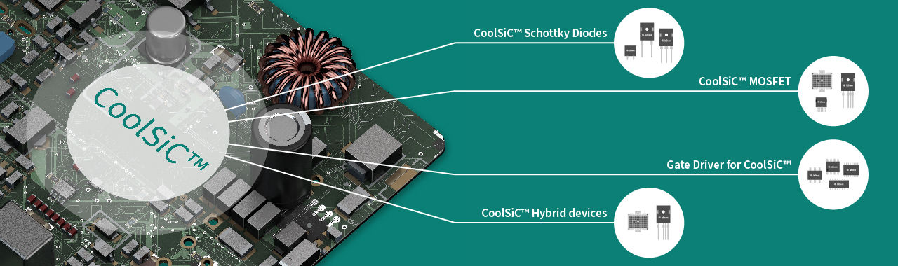
CoolSiC™ technology details
Discover more about Silicon Carbide solution offered by Infineon

Our overall goal is to combine the low RDS(on) offered by silicon carbide MOSFETs with an gate drive mode in which the device operates in the safe oxide field-strength conditions. Consequently, it was decided to focus on trench-based devices moving away from a planar surface with high-defect density towards more favorable surface orientations. The latter enabling a low channel resistance at low oxide fields. These boundary conditions are the baseline for transferring quality assurance methodologies established in the silicon power semiconductor world in order to guarantee FIT rates expected in industrial and even automotive applications.
SiC devices operate at much higher drain-induced electric fields in the blocking mode compared to their Si counterparts (MV instead of kV). Thus, high electric fields in the oxide in the on-state AND off state can potentially accelerate the wear-out. For off state stress protection by deep p-regions is adopted, for on-state a thick oxide is used in order to circumvent the limits to screen remaining extrinsic oxide defects for thin oxides.
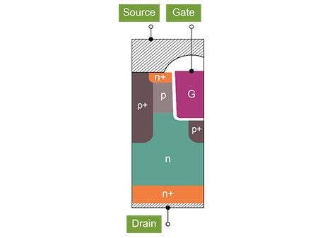
The CoolSiC™ MOSFET trench concept is optimized for the operation of the body diode. The trench bottom embedded into a p+ region enhances the body diode area.
The CoolSiC™ MOSFET cell design was developed to limit the electric field in the gate oxide in on-state as well as in off-state to maintain reliability. Additionally, for all variants a low on-resistance, stable and reproducible even in mass production, is achieved. Guaranteed at driving voltage levels of only VGS= 15 V combined with a sufficiently high gate-source-threshold voltage of typically 4.5 V, being a benchmark in the field of SiC transistors.
Balancing primary perfomance indicators and other relevant aspects for power electronic designs
CoolSiC™ is synonymous with pioneering in trench SiC MOSFET technology. Infineon once again demonstrates that we continue to strive for innovation and technology leadership – also in the WBG arena. What we offer and the way we offer it, differentiates us.
The CoolSiC™ MOSFET features superior performance in terms of switching behavior and total losses. One of the highlights is the possibility to turn off the device with zero gate bias, which makes the CoolSiC™ transistor concept the only true “normally-off” device in the market at the moment.
In addition to superior gate oxide reliability and a stable, robust body diode is a key feature of CoolSiC ™ MOSFETs when being compared to currently available SiC MOSFETs.
Hard-switching topologies
- Lowest switching losses at fast switching speed
- Easy design-in thanks to robustness against parasitic turn-on effects (low over- / under-voltages)
- Short-circuit rating 3 µs (relevant in e.g. servo drives)
Soft-switching topologies
- Lowest switching losses and easy design-in
- 0 V turn-off can be applied, critical e.g., for LLC and ZVS designers having design experience with SJ MOSFETs (e.g., Infineon’s CoolMOS™) operated with 0 V turn-off
Body diode – An integral part
In contrast to IGBT’s a vertical MOSFET like the CoolSiC™ device offers conduction in reverse mode (via the body diode). Thus, it can be used as a freewheeling diode. However, due to the bandgap of SiC, the knee voltage of this diode is relatively high (around 3 V).
All CoolSiC™ MOSFETs– either packaged in Infineon’s SiC-modules or belonging to Infineon’s SiC-discrete portfolio - have an integrated body diode. An additional Schottky diode is not required.
The diode is usable for typical freewheeling functions. Also, it can be used without a Schottky barrier diode (SBD). It is mandatory to use synchronous rectification (turn on the channel in diode mode after a short dead time) to benefit from low conduction losses.
The CoolSiC™ MOSFET body diode is rated for hard commutation and is highly robust, withstanding 7x Inom 10 ms surge current. It proves to be long-term stable and does not drift beyond the datasheet limits. Infineon ensures device parameters - RDS(on) and VSD - stay within datasheet limitation for the operation lifetime by adhering to:
- Optimized screening process for the reduction of defect density
- 100% final clearance testing (FCT) verifying the low DPM rate
Share in WeChat
Scan the QR code with your WeChat App to share this page.
Infineon is the world’s first commercial Silicon Carbide (SiC) device supplier. Long market presence and experience enable Infineon to deliver highly reliable, industry-leading SiC performance. The differences in material properties between Silicon Carbide and Silicon limit the fabrication of practical Silicon unipolar diodes (Schottky diodes) to a range up to 100 V–150 V, with relatively high on-state resistance and leakage current. In SiC material Schottky diodes can reach a much higher breakdown voltage. The Infineon portfolio of Silicon Carbide (SiC) products covers 600 V and 650 V to 1200 V Schottky diodes.
The combination of a Silicon-based switch and a CoolSiC™ schottky diode is called a “hybrid solution”.
Compared to Silicon IGBT solutions, the turn-on losses can be reduced. In addition higher switching frequency and higher current handling capability can be realized. Highest power density and efficiency can be achieved by using the chips as standalone components or in combination with silicon power devices in power modules. SiC diodes in particular are enabling parts to further extend the capabilities of IGBT technology.
More about CoolSiC™ Hybrid Modules
The hybrid modules in the well-known EasyPACK™ come in booster as well as 3-level configuration. The portfolio consists of power modules where SiC diodes and IGBT chips form an ideal pair leveraging the best available performance in the targeted applications, such as solar energy systems.
The number of power modules with SiC components will be complemented step by step with further parts, using either the combination of SiC diodes with silicon transistors or even SiC based transistors, currently based on the awarded CoolSiC™ technology. No matter the power of the application, our power module SiC portfolio enables a more efficient design, ranging from packages like EasyPACK™ 1B/2B to larger packages like EasyPACK™ 3B.
More about CoolSiC™ Hybrid Discretes
CoolSiC™ Hybrid Discretes are a combination of two established, best-in-class semiconductor technologies: 650 V TRENCHSTOP™ 5 IGBTs and CoolSiC™ Schottky diodes G6. The resulting products have a performance similar to silicon carbide switches but come at an attractive price.
In case of SiC to reduce FIT rates (quantifying hard fails) - two influencing factors must be considered:
- Cosmic ray effects (same as for Si devices)
- Gate oxide reliability (due to the oxide field stress)
Cosmic ray stability is usually achieved by optimizing the electric field distribution in the drift zone. However, to bring oxide FIT rates down, effective screening of electrically active defects is required. Principally, Si and SiC MOSFETs have pretty much the same intrinsic oxide lifetime as long as the devices do not contain defect-related impurities, i.e. extrinsic defects. SiC MOSFETs exhibit a much higher extrinsic defect density in the gate oxide, in contrast to Si MOSFETs. Devices with extrinsic defects break down earlier in comparison to defect-free devices. The challenge to guarantee sufficient reliability of the gate oxide of SiC MOSFETs is to reduce the number of devices being affected by extrinsics by means of electrical screening. Each device is subjected to a gate stress pattern - destroying those with critical extrinsics. As a consequence, the enabler for an efficient gate oxide screening is a nominal oxide thickness that is much higher than is typically needed to fulfill the intrinsic lifetime targets, what leads to a trade-off between gate-oxide-FIT-rate and device performance.

To further improve its SiC technology, Infineon invested a lot into testing on-state oxide reliability of electrically screened SiC MOSFETs and the off state oxide stress due to the electric field conditions in SiC power devices.
Today we can claim:
- Due to the optimized gate oxide thickness our gate oxide screening is more efficient compared to competing SiC MOSFET manufacturers.
- Lower gate oxide failure rates during the lifetime and no early failures translate into the highest possible gate oxide quality at the customer side.
In 2018 Infineon acquired the Startup SILTECTRA™ to integrate innovative laser-based material separation technologies to the thin wafer technology competence. The SILTECTRA™ COLD SPLIT technology splits crystalline materials like Silicon Carbide with minimal loss of material compared to common sawing technologies.
How silicon carbide fuels rail tech | Ask the Expert
Can silicon carbide help drive innovation in rail transportation?
In this episode of “Ask the Expert”, our expert Sebastian explains how silicon carbide enables more efficient and compact traction converters, supporting rail transportation's electrification and decarbonization.
Value proposition of SiC: basics – Module 1
For more than twenty years, Infineon has been at the forefront of developing solutions addressing demands for energy savings, size reduction, system integration and improved reliability in its products. One of the most revolutionary developments was the use of SiC as a main compound in some of its devices. Infineon is the world’s first SiC discrete power supplier. It was the global pioneer in SiC technology and commercialization. In this training we will present one of the most successful solutions that Infineon’s developed in this field.
Value proposition of SiC: basics – Module 2
For more than twenty years, Infineon has been at the forefront of developing solutions addressing demands for energy savings, size reduction, system integration and improved reliability in its products. One of the most revolutionary developments was the use of SiC as a main compound in some of its devices. Infineon is the world’s first SiC discrete power supplier. It was the global pioneer in SiC technology and commercialization. In this training we will present one of the most successful solutions that Infineon’s developed in this field.
5 minutes - 5 reasons why SiC
To lead the transformation towards sustainable energy generation and consumption, you know that silicon carbide technology is at the strategic core to address key market trends in this direction. To do so, here are five reasons why you should choose Infineon’s SiC devices.
CoolSiC™ – Customer Success Stories
This video highlights the benefits of CoolSiC™, as seen through the eyes of our customers. Featuring testimonials from alpitronic, Tritium, Lite-On, Siemens Mobility, and Fronius, we see how SiC is driving innovation in energy generation, storage, and consumption.
Cold Split Technology
CoolSiC™ trench technology – a revolution to rely on
SiC power semiconductors in real designs – DC-link connection
Introduction to SiC reliability
This training covers the properties of Silicon Carbide which change the way how an inverter is designed compared to Si-chips. With that in mind, we explain SiC specific degradation mechanisms and how to ensure that SiC devices survive in the application, considering these special failure modes, by applying the reliability tests Infineon developed. These are internally mandatory for SiC device qualifications to ensure better quality, safety, and reliable device performance for years.
Share in WeChat
Scan the QR code with your WeChat App to share this page.