
- ASIC
- Battery management ICs
- Clocks and timing solutions
- ESD and surge protection devices
- Automotive Ethernet
- Evaluation Boards
- High reliability
- Isolation
- Memories
- Microcontroller
- Power
- RF
- Security and smart card solutions
- Sensor technology
- Small signal transistors and diodes
- Transceivers
- Universal Serial Bus (USB)
- Wireless connectivity
- Search Tools
- Technology
- Packages
- Product Information
- Ordering
- Overview
- Automotive Ethernet PHY for in-vehicle networking
- Automotive Ethernet Switches for in-vehicle networking
- Overview
- Embedded flash IP solutions
- Flash+RAM MCP solutions
- F-RAM (Ferroelectric RAM)
- NOR flash
- nvSRAM (non-volatile SRAM)
- PSRAM – Pseudostatic RAM
- Radiation hardened and high-reliability memories
- SRAM (static RAM)
- Wafer and die memory solutions
- Overview
- 32-bit FM Arm® Cortex® Microcontroller
- 32-bit AURIX™ TriCore™ microcontroller
- 32-bit PSOC™ Arm® Cortex® microcontroller
- 32-bit TRAVEO™ T2G Arm® Cortex® microcontroller
- 32-bit XMC™ industrial microcontroller Arm® Cortex®-M
- Legacy microcontroller
- Motor control SoCs/SiPs
- Sensing controllers
- Overview
- AC-DC power conversion
- Automotive conventional powertrain ICs
- Class D audio amplifier ICs
- Contactless power and sensing ICs
- DC-DC converters
- Diodes and thyristors (Si/SiC)
- Gallium nitride (GaN)
- Gate driver ICs
- IGBTs – Insulated gate bipolar transistors
- Intelligent power modules (IPM)
- LED driver ICs
- Motor drivers
- MOSFETs
- Power modules
- Power supply ICs
- Protection and monitoring ICs
- Silicon carbide (SiC)
- Smart power switches
- Solid state relays
- Wireless charging ICs
- Overview
- Antenna cross switches
- Antenna tuners
- Bias and control
- Coupler
- Driver amplifiers
- Rad hard microwave and RF
- Low noise amplifiers (LNAs)
- RF diode
- RF switches
- RF transistors
- Wireless control receiver
- Overview
- Calypso® products
- CIPURSE™ products
- Contactless memories
- OPTIGA™ embedded security solutions
- SECORA™ security solutions
- Security controllers
- Smart card modules
- Smart solutions for government ID
- Overview
- ToF 3D image sensors
- Current sensors
- Gas sensors
- Inductive position sensors
- MEMS microphones
- Pressure sensors
- Radar sensors
- Magnetic position sensors
- Magnetic speed sensors
- Overview
- Bipolar transistors
- Diodes
- Small signal/small power MOSFET
- Overview
- Automotive transceivers
- Control communication
- Powerline communications
- Overview
- USB 2.0 peripheral controllers
- USB 3.2 peripheral controllers
- USB hub controllers
- USB PD high-voltage microcontrollers
- USB-C AC-DC and DC-DC charging solutions
- USB-C charging port controllers
- USB-C Power Delivery controllers
- Overview
- AIROC™ Automotive wireless
- AIROC™ Bluetooth® and multiprotocol
- AIROC™ connected MCU
- AIROC™ Wi-Fi + Bluetooth® combos
- Overview
- Commercial off-the-shelf (COTs) memory portfolio
- Defense memory portfolio
- High-reliability power conversion and management
- Overview
- Rad hard microwave and RF
- Radiation hardened power
- Space memory portfolio
- Overview
- Parallel NOR flash
- SEMPER™ NOR flash family
- SEMPER™ X1 LPDDR flash
- Serial NOR flash
- Overview
- FM0+ 32-bit Arm® Cortex®-M0+ microcontroller (MCU) families
-
FM3 32-bit Arm® Cortex®-M3 microcontroller (MCU) families
- Overview
- FM3 CY9AFx1xK series Arm® Cortex®-M3 microcontroller (MCU)
- FM3 CY9AFx1xL/M/N series Arm® Cortex®-M3 microcontroller (MCU)
- FM3 CY9AFx2xK/L series Arm® Cortex®-M3 microcontroller (MCU)
- FM3 CY9AFx3xK/L series ultra-low leak Arm® Cortex®-M3 microcontroller (MCU)
- FM3 CY9AFx4xL/M/N series low power Arm® Cortex®-M3 microcontroller (MCU)
- FM3 CY9AFx5xM/N/R series low power Arm® Cortex®-M3 microcontroller (MCU)
- FM3 CY9AFxAxL/M/N series ultra-low leak Arm® Cortex®-M3 microcontroller (MCU)
- FM3 CY9BFx1xN/R high-performance series Arm® Cortex®-M3 microcontroller (MCU)
- FM3 CY9BFx1xS/T high-performance series Arm® Cortex®-M3 microcontroller (MCU)
- FM3 CY9BFx2xJ series Arm® Cortex®-M3 microcontroller (MCU)
- FM3 CY9BFx2xK/L/M series Arm® Cortex®-M3 microcontroller (MCU)
- FM3 CY9BFx2xS/T series Arm® Cortex®-M3 microcontroller (MCU)
-
FM4 32-bit Arm® Cortex®-M4 microcontroller (MCU) families
- Overview
- FM4 CY9BFx6xK/L high-performance series Arm® Cortex®-M4F microcontroller (MCU)
- FM4 CY9BFx6xM/N/R high-performance series Arm® Cortex®-M4F microcontroller (MCU)
- FM4 S6E2C high-performance series Arm® Cortex®-M4F microcontroller (MCU)
- FM4 S6E2G series connectivity Arm® Cortex®-M4F microcontroller (MCU)
- FM4 S6E2H high-performance series Arm® Cortex®-M4F microcontroller (MCU)
- Overview
-
32-bit TriCore™ AURIX™ – TC2x
- Overview
- AURIX™ family – TC21xL
- AURIX™ family – TC21xSC (wireless charging)
- AURIX™ family – TC22xL
- AURIX™ family – TC23xL
- AURIX™ family – TC23xLA (ADAS)
- AURIX™ family – TC23xLX
- AURIX™ family – TC264DA (ADAS)
- AURIX™ family – TC26xD
- AURIX™ family – TC27xT
- AURIX™ family – TC297TA (ADAS)
- AURIX™ family – TC29xT
- AURIX™ family – TC29xTT (ADAS)
- AURIX™ family – TC29xTX
- AURIX™ TC2x emulation devices
-
32-bit TriCore™ AURIX™ – TC3x
- Overview
- AURIX™ family - TC32xLP
- AURIX™ family – TC33xDA
- AURIX™ family - TC33xLP
- AURIX™ family – TC35xTA (ADAS)
- AURIX™ family – TC36xDP
- AURIX™ family – TC37xTP
- AURIX™ family – TC37xTX
- AURIX™ family – TC38xQP
- AURIX™ family – TC39xXA (ADAS)
- AURIX™ family – TC39xXX
- AURIX™ family – TC3Ex
- AURIX™ TC37xTE (emulation devices)
- AURIX™ TC39xXE (emulation devices)
- 32-bit TriCore™ AURIX™ – TC4x
- Overview
- PSOC™ 4 Arm® Cortex®-M0/M0+
- PSOC™ 4 HV Arm® Cortex®-M0+
- PSOC™ 5 LP Arm® Cortex®-M3
- PSOC™ 6 Arm® Cortex®-M4/M0+
- PSOC™ Multitouch Touchscreen Controller
- PSOC™ Control C3 Arm® Cortex®-M33
- PSOC™ Automotive 4: Arm® Cortex®-M0/M0+
- PSOC™ Edge Arm® Cortex® M55/M33
- Overview
- 32-bit TRAVEO™ T2G Arm® Cortex® for body
- 32-bit TRAVEO™ T2G Arm® Cortex® for cluster
- Overview
- 32-bit XMC1000 industrial microcontroller Arm® Cortex®-M0
- 32-bit XMC4000 industrial microcontroller Arm® Cortex®-M4
- XMC5000 Industrial Microcontroller Arm® Cortex®-M4F
- 32-bit XMC7000 Industrial Microcontroller Arm® Cortex®-M7
- Overview
- Legacy 32-bit MCU
- Legacy 8-bit/16-bit microcontroller
- Other legacy MCUs
- Overview
- AC-DC integrated power stage - CoolSET™
- AC-DC PWM-PFC controller
- Overview
- Bridge rectifiers & AC switches
- CoolSiC™ Schottky diodes
- Diode bare dies
- Silicon diodes
- Thyristor / Diode Power Modules
- Thyristor soft starter modules
- Thyristor/diode discs
- Overview
- Automotive gate driver ICs
- EiceDRIVER™ SiC MOSFET gate driver ICs
- Isolated Gate Driver ICs
- Gate driver ICs for GaN HEMTs
- Half-bridge drivers
- High side gate drivers
- Level-Shift Gate Driver ICs
- Low-Side Drivers
- Three phase drivers
- Transformer Driver ICs
- Overview
- AC-DC LED driver ICs
- Ballast IC
- DC-DC LED driver IC
- LED dimming interface IC
- Linear LED driver IC
- LITIX™ - Automotive LED Driver IC
- NFC wireless configuration IC with PWM output
- VCSEL driver
- Overview
- BLDC motor drivers
- BDC motor drivers
- Stepper & servo motor drivers
- Motor drivers with MCU
- Bridge drivers with MOSFETs
- Gate driver ICs
- Overview
- Automotive MOSFET
- Dual MOSFETs
- MOSFET (Si & SiC) Modules
- N-channel depletion mode MOSFET
- N-channel MOSFETs
- P-channel MOSFETs
-
Silicon carbide CoolSiC™ MOSFETs
- Overview
- Silicon Carbide MOSFET modules
- Silicon carbide MOSFET discretes
- Silicon carbide MOSFETs bare dies
- 400 V / 440 V Silicon Carbide MOSFETs
- 650 V Silicon Carbide MOSFETs
- 750 V Silicon Carbide MOSFETs
- 1200 V Silicon Carbide MOSFETs
- 2000 V Silicon Carbide MOSFETs
- 2300 V Silicon Carbide MOSFETs
- 3300 V Silicon Carbide MOSFETs
- 1700 V Silicon Carbide MOSFETs
- Small signal/small power MOSFET
- Overview
- IGBT modules
- MOSFET (Si & SiC) Modules
- Intelligent power modules (IPM)
- Diodes and thyristors (Si/SiC)
- Automotive IGBT and CoolSiC™ MOSFET modules
- High density power modules
- Overview
- Automotive transceivers
- Linear voltage regulators for automotive applications
- OPTIREG™ PMIC
- OPTIREG™ switcher
- OPTIREG™ System Basis Chips (SBC)
- Overview
- eFuse
- High-side switches
- Low-side switches
- Multichannel SPI Switches & Controller
- Overview
- Radar sensors for automotive
- Radar sensors for IoT
- Overview
- EZ-USB™ CX3 MIPI CSI2 to USB 3.0 camera controller
- EZ-USB™ FX10 & FX5N USB 10Gbps peripheral controller
- EZ-USB™ FX20 USB 20 Gbps peripheral controller
- EZ-USB™ FX3 USB 5 Gbps peripheral controller
- EZ-USB™ FX3S USB 5 Gbps peripheral controller with storage interface
- EZ-USB™ FX5 USB 5 Gbps peripheral controller
- EZ-USB™ SD3 USB 5 Gbps storage controller
- EZ-USB™ SX3 FIFO to USB 5 Gbps peripheral controller
- Overview
- EZ-PD™ CCG3 USB type-C port controller PD
- EZ-PD™ CCG3PA USB-C and PD
- EZ-PD™ CCG3PA-NFET USB-C PD controller
- EZ-PD™ CCG7x consumer USB-C Power Delivery & DC-DC controller
- EZ-PD™ PAG1: power adapter generation 1
- EZ-PD™ PAG2: Power Adapter Generation 2
- EZ-PD™ PAG2-PD USB-C PD Controller
- Overview
- EZ-PD™ ACG1F one-port USB-C controller
- EZ-PD™ CCG2 USB Type-C port controller
- EZ-PD™ CCG3PA Automotive USB-C and Power Delivery controller
- EZ-PD™ CCG4 two-port USB-C and PD
- EZ-PD™ CCG5 dual-port and CCG5C single-port USB-C PD controllers
- EZ-PD™ CCG6 one-port USB-C & PD controller
- EZ-PD™ CCG6_CFP and EZ-PD™ CCG8_CFP Dual-Single-Port USB-C PD
- EZ-PD™ CCG6DF dual-port and CCG6SF single-port USB-C PD controllers
- EZ-PD™ CCG7D Automotive dual-port USB-C PD + DC-DC controller
- EZ-PD™ CCG7S Automotive single-port USB-C PD solution with a DC-DC controller + FETs
- EZ-PD™ CCG8 dual-single-port USB-C PD
- EZ-PD™ CMG1 USB-C EMCA controller
- EZ-PD™ CMG2 USB-C EMCA controller with EPR
- LATEST IN
- Aerospace and defense
- AI and data center
- Automotive
- Communications
- Consumer electronics
- Health and lifestyle
- Home appliances
- Industrial
- Security solutions
- Smart home and building
- Solutions
- Overview
- Defense applications
- Space applications
- Overview
- Data center power solutions
- Edge computing
- Machine Learning Edge AI
- Overview
- ADAS & autonomous driving
- Automotive body electronics & power distribution
- Automotive LED lighting systems
- Chassis control & safety
- Electric vehicle drivetrain system
- EV thermal management system
- In-vehicle infotainment & HMI
- Light electric vehicle solutions
- Overview
- Satellite communications
- Telecommunications infrastructure
- Overview
- Power adapters and chargers
- Complete system solutions for smart TVs
- Mobile device and smartphone solutions
- Power tools
- Semiconductor solutions for home entertainment applications
- Smart conference systems
- Multicopters and drones
- AR and smart glasses
- Overview
- Power adapters and chargers
- Asset Tracking
- Battery formation and testing
- Electric forklifts
- Battery energy storage (BESS)
- EV charging
- High voltage solid-state power distribution
- Industrial automation
- Industrial motor drives and controls
- Industrial robots
- LED lighting system design
- Light electric vehicle solutions
- Power tools
- Power transmission and distribution
- Traction
- Uninterruptible power supplies (UPS)
- Digital health
- Robotics
- Wind power
- Hydrogen electrolysis
- Renewables
- Photovoltaic
- Industrial power supplies
- Overview
- Device authentication and brand protection
- Embedded security for the Internet of Things (IoT)
- eSIM applications
- Government identification
- Mobile security
- Payment solutions
- Access control and ticketing
- Overview
- Domestic robots
- Heating ventilation and air conditioning (HVAC)
- Home and building automation
- PC accessories
- Semiconductor solutions for home entertainment applications
- Overview
- Battery management systems (BMS)
- Connectivity
- Human Machine Interface
- Machine Learning Edge AI
- Motor control
- Power conversion
- Security
- Sensor solutions
- System diagnostics and analytics
- Overview
- FPGAs in datacenter applications
- Power system reliability modeling
-
Server rack power management
- Overview
- Server power supply units (PSU)
- Server battery backup units (BBU)
- Medium voltage IBC (48 V)
- Ampere CPU voltage regulator Ics
- Intel CPU voltage regulator Ics
- AMD CPU voltage regulator Ics
- AI accelerator cards
- SmartNIC cards
- Network switches for AI data centers and server racks
- Server power path protection
- Data center power distribution
- Overview
- Automotive auxiliary systems
- Automotive gateway
- Automotive power distribution
- Body control modules (BCM)
- Comfort & convenience electronics
- Zonal DC-DC converter 48 V-12 V
- Zone control unit
- Overview
- Automotive animated LED lighting system
- Automotive LED front single light functions
- Automotive LED rear single light functions
- Full LED headlight system - multi-channel LED driver
- LED drivers (electric two- & three-wheelers)
- LED pixel light controller - supply & communication
- Static interior ambient LED light
- Overview
- Active suspension control
- Automotive braking solutions
- Automotive steering solutions
- Chassis domain control
- Overview
-
Automotive BMS
- Overview
- Automotive battery cell monitoring & balancing
- Automotive battery control unit (BCU)
- Automotive battery isolated communication
- Automotive battery management system (BMS) - 12 V to 24 V
- Automotive battery management system (BMS) - 48 V
- Automotive battery management system (BMS) - high-voltage
- Automotive battery pack monitoring
- Automotive battery passport & event logging
- Automotive battery protection & disconnection
- Automotive current sensing & coulomb counting
- BMS (electric two- & three-wheelers)
- EV charging
- EV inverters
- EV power conversion & OBC
- FCEV powertrain system
- Overview
- AC-DC power conversion for telecommunications infrastructure
- DC-DC power conversion for telecommunications infrastructure
- FPGA in wired and wireless telecommunications applications
- Power system reliability modeling
- RF front end components for telecommunications infrastructure
- Memory solutions for cellular base stations
- Security solutions for cellular base stations
- Overview
- Audio amplifier solutions
- Complete system solutions for smart TVs
- Distribution audio amplifier unit solutions
- Home theater installation speaker system solutions
- Party speaker solutions
- PoE audio amplifier unit solutions
- Portable speaker solutions
- Powered active speaker systems
- Remote control
- Smart speaker designs
- Soundbar solutions
- Overview
- Data center power solutions
- Digital input/output (I/O) modules
- DIN rail power supply solutions
- Home and building automation
- Industrial HMI Monitors and Panels
- Industrial motor drives and controls
- Industrial PC
- Industrial robots
- Machine vision
- Mobile robots (AGV, AMR)
- Programmable logic controller (PLC)
- Solid-state circuit breaker (SSCB)
- Uninterruptible power supplies (UPS)
- Overview
- Durable healthcare equipment
- Disposable healthcare equipment
- Healthcare wearables
- Overview
- Automotive BMS
- Industrial and consumer BMS
- Overview
- AC-DC power conversion
- DC-DC power conversion
- Overview
- Power supply health monitoring
- LATEST IN
- Digital documentation
- Boards & Kits
- Finder & selection tools
- Platforms
- Services
- Simulation & Modeling
- Software
- Tools
- Partners
- Infineon for Makers
- University Alliance Program
- Overview
- Bipolar Discs Finder
- Bipolar Module Finder
- Connected Secure Systems Finder
- Diode Rectifier Finder
- ESD Protection Finder
- Evaluation Board Finder
- Gate Driver Finder
- IGBT Discrete Finder
- IGBT Module Finder
- IPM Finder
- Microcontroller Finder
- MOSFET Finder
- PMIC Finder
- Product Finder
- PSOC™ and FMx MCU Board & Kit Finder
- Radar Finder
- Reference Design Finder
- Simulation Model Finder
- Smart Power Switch Finder
- Transceiver Finder
- Voltage Regulator Finder
- Wireless Connectivity Board & Kit Finder
- Overview
- AIROC™ software & tools
- AURIX™ software & tools
- DRIVECORE for automotive software development
- iMOTION™ software & tools
- Infineon Smart Power Switches & Gate Driver Tool Suite
- MOTIX™ software & tools
- OPTIGA™ software & tools
- PSOC™ software & tools
- TRAVEO™ software & tools
- XENSIV™ software & tools
- XMC™ software & tools
- Overview
- CoolGaN™ Simulation Tool (PLECS)
- HiRel Fit Rate Tool
- Infineon Designer
- Interactive product sheet
- IPOSIM Online Power Simulation Platform
- InfineonSpice Offline Simulation Tool
- OPTIREG™ automotive power supply ICs Simulation Tool (PLECS)
- Power MOSFET Simulation Models
- PowerEsim Switch Mode Power Supply Design Tool
- Solution Finder
- XENSIV™ Magnetic Sensor Simulation Tool
- Overview
- AURIX™ certifications
- AURIX™ development tools
-
AURIX™ Embedded Software
- Overview
- AURIX™ Applications software
- AURIX™ Artificial Intelligence
- AURIX™ Gateway
- AURIX™ iLLD Drivers
- Infineon safety
- AURIX™ Security
- AURIX™ TC3xx Motor Control Application Kit
- AURIX™ TC4x SW application architecture
- Infineon AUTOSAR
- Communication and Connectivity
- Middleware
- Non AUTOSAR OS/RTOS
- OTA
- AURIX™ Microcontroller Kits
- Overview
- TRAVEO™ Development Tools
- TRAVEO™ Embedded Software
- Overview
- XENSIV™ Development Tools
- XENSIV™ Embedded Software
- XENSIV™ evaluation boards
- Overview
- CAPSENSE™ Controllers Code Examples
- Memories for Embedded Systems Code Examples
- PSOC™ 1 Code Examples for PSOC™ Designer
- PSOC™ 3 Code Examples for PSOC™ Creator
- PSOC™ 3/4/5 Code Examples
- PSOC™ 4 Code Examples for PSOC™ Creator
- PSOC™ 6 Code Examples for PSOC™ Creator
- PSOC™ 63 Code Examples
- USB Controllers Code Examples
- Overview
- DEEPCRAFT™ AI Hub
- DEEPCRAFT™ Audio Enhancement
- DEEPCRAFT™ Model Converter
-
DEEPCRAFT™ Ready Models
- Overview
- DEEPCRAFT™ Ready Model for Baby Cry Detection
- DEEPCRAFT™ Ready Model for Cough Detection
- DEEPCRAFT™ Ready Model for Direction of Arrival (Sound)
- DEEPCRAFT™ Ready Model for Factory Alarm Detection
- DEEPCRAFT™ Ready Model for Fall Detection
- DEEPCRAFT™ Ready Model for Gesture Classification
- DEEPCRAFT™ Ready Model for Siren Detection
- DEEPCRAFT™ Ready Model for Snore Detection
- DEEPCRAFT™ Studio
- DEEPCRAFT™ Voice Assistant
- Overview
- AIROC™ Wi-Fi & Bluetooth EZ-Serial Module Firmware Platform
- AIROC™ Wi-Fi & Bluetooth Linux and Android Drivers
- emWin Graphics Library and GUI for PSOC™
- Infineon Complex Device Driver for Battery Management Systems
- Memory Solutions Hub
- PSOC™ 6 Peripheral Driver Library (PDL) for PSOC™ Creator
- USB Controllers EZ-USB™ GX3 Software and Drivers
- Overview
- CAPSENSE™ Controllers Configuration Tools EZ-Click
- DC-DC Integrated POL Voltage Regulators Configuration Tool – PowIRCenter
- EZ-USB™ SX3 Configuration Utility
- FM+ Configuration Tools
- FMx Configuration Tools
- Tranceiver IC Configuration Tool
- USB EZ-PD™ Configuration Utility
- USB EZ-PD™ Dock Configuration Utility
- USB EZ-USB™ HX3C Blaster Plus Configuration Utility
- USB UART Config Utility
- XENSIV™ Tire Pressure Sensor Programming
- Overview
- EZ-PD™ CCGx Dock Software Development Kit
-
FMx Softune IDE
- Overview
- RealOS™ Real-Time Operating System
- Softune IDE Language tools
- Softune Workbench
- Tool Lineup for F2MC-16 Family SOFTUNE V3
- Tool Lineup for F2MC-8FX Family SOFTUNE V3
- Tool Lineup for FR Family SOFTUNE V6
- Virtual Starter Kit
- Windows 10 operation of released SOFTUNE product
- Windows 7 operation of released SOFTUNE product
- Windows 8 operation of released SOFTUNE product
- ModusToolbox™ Software
- PSOC™ Creator Software
- Radar Development Kit
- RUST
- USB Controllers SDK
- Wireless Connectivity Bluetooth Mesh Helper Applications
- XMC™ DAVE™ Software
- Overview
- AIROC™ Bluetooth® Connect App Archive
- Cypress™ Programmer Archive
- EZ-PD™ CCGx Power Software Development Kit Archive
- ModusToolbox™ Software Archive
- PSOC™ Creator Archive
- PSOC™ Designer Archive
- PSOC™ Programmer Archive
- USB EZ-PD™ Configuration Utility Archives
- USB EZ-PD™ Host SDK Archives
- USB EZ-USB™ FX3 Archive
- USB EZ-USB™ HX3PD Configuration Utility Archive
- WICED™ Smart SDK Archive
- WICED™ Studio Archive
- Overview
- Infineon Developer Center Launcher
- Infineon Register Viewer
- Pin and Code Wizard
- Timing Solutions
- Wireless Connectivity
- LATEST IN
- Support
- Training
- Developer Community
- News
Business & Financial Press
May 20, 2026
Business & Financial Press
May 11, 2026
Business & Financial Press
May 07, 2026
Quarterly Report
May 06, 2026
- Company
- Our stories
- Events
- Press
- Investor
- Careers
- Quality
- Latest news
Business & Financial Press
May 20, 2026
Business & Financial Press
May 11, 2026
Business & Financial Press
May 07, 2026
Quarterly Report
May 06, 2026
Content could not be loaded
Unfortunately, we were unable to load the content for this section. You may want to refresh the page or try again later.
Product details
-
ClassificationISO 26262-compliant
-
Density2 GBit
-
FamilyHS-T
-
Interface Bandwidth333 MByte/s
-
Interface Frequency (SDR/DDR) (MHz)166 / 166
-
InterfacesOctal
-
Lead Ball FinishSn/Ag/Cu
-
Operating Temperature range-40 °C to 105 °C
-
Operating Voltage range1.7 V to 2 V
-
Operating Voltage1.8 V
-
Peak Reflow Temp260 °C
-
Planned to be available until at least2037
-
QualificationAutomotive
| Recommended | ||
|
OPN
|
S28HS02GTFPBHB150 | |
| Product Status | active and preferred | |
| Infineon Package | ||
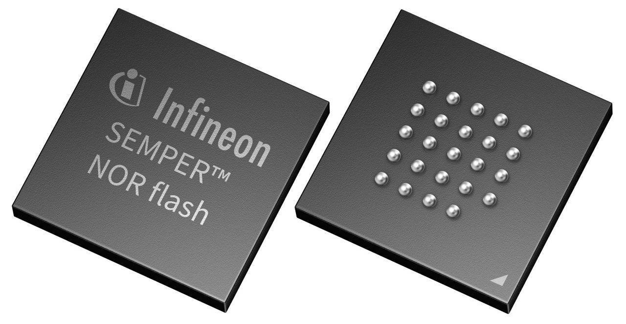
| Package Name | FBGA-24 (002-24801) | |
| Packing Size | 2600 | |
| Packing Type | TRAY | |
| Moisture Level | 3 | |
| Moisture Packing | DRY | |
| Lead-free | Yes | |
| Halogen Free | Yes | |
| RoHS Compliant | Yes | |
|
Infineon stock last updated:
|
||
|
|
||
|
|
| Product Status |
Active
|
|---|---|
| Infineon Package | |
| Package Name | FBGA-24 (002-24801) |
| Packing Size | 2600 |
| Packing Type | TRAY |
| Moisture Level | 3 |
| Moisture Packing | DRY |
| Lead Free | |
| Halogen Free | |
| RoHS Compliant | |
Features
- 45-nm MIRRORBIT™ stores 2 bits/cell
- JEDEC JESD251 xSPI compliant
- Octal OPI supports SDR and DDR
- Legacy ×1 SPI supports SDR
- Data strobe (DS) for read capture
- Burst reads: wrapped or linear
- Uniform or hybrid sector architecture
- Configurable 256/512-byte prog buf
- OTP secure array 1024 bytes
- ECC SECDED on array data
- CRC detects memory array errors
- SafeBoot init/config recovery
Benefits
- Higher density in same die area
- Easier host compatibility via xSPI
- Higher read throughput in OPI
- Backward compatible SPI designs
- Simplifies high-speed timing margin
- Efficient streaming or page reads
- Optimizes erase granularity for FW
- Faster program throughput option
- Secure storage for keys/IDs
- Improves data reliability in field
- Detects corruption for safe action
- Improves boot robustness, recovery