- ASIC
- Battery management ICs
- Clocks and timing solutions
- ESD and surge protection devices
- Automotive Ethernet
- Evaluation Boards
- High reliability
- Isolation
- Memories
- Microcontroller
- Power
- RF
- Security and smart card solutions
- Sensor technology
- Small signal transistors and diodes
- Transceivers
- Universal Serial Bus (USB)
- Wireless connectivity
- Search Tools
- Technology
- Packages
- Product Information
- Ordering
- Overview
- Automotive Ethernet PHY for in-vehicle networking
- Automotive Ethernet Switches for in-vehicle networking
- Overview
- Embedded flash IP solutions
- Flash+RAM MCP solutions
- F-RAM (Ferroelectric RAM)
- NOR flash
- nvSRAM (non-volatile SRAM)
- PSRAM – Pseudostatic RAM
- Radiation hardened and high-reliability memories
- SRAM (static RAM)
- Wafer and die memory solutions
- Overview
- AURIX™ TriCore™ MCUs
- PSOC™ MCUs
- TRAVEO™ T2G MCUs
- XMC™ MCUs
- Legacy MCUs
- MOTIX™ motor control SoCs/SIPs
- Overview
- AC-DC power conversion
- Automotive conventional powertrain ICs
- Class D audio amplifier ICs
- Contactless power and sensing ICs
- DC-DC converters
- Diodes and thyristors (Si/SiC)
- eFuses
- Gallium nitride (GaN)
- Gate Driver ICs
- IGBTs – Insulated gate bipolar transistors
- Intelligent power modules (IPM)
- JFETs
- LED driver ICs
- Motor drivers
- MOSFETs
- Power modules
- Power supply ICs
- Protection and monitoring ICs
- Silicon carbide (SiC)
- Smart power switches
- Solid state relays and isolators
- Wireless charging ICs
- Overview
- Antenna cross switches
- Antenna tuners
- Bias and control
- Coupler
- Driver amplifiers
- Rad hard microwave and RF
- Low noise amplifiers (LNAs)
- RF diode
- RF switches
- RF transistors
- Wireless control receiver
- Overview
- Calypso® products
- CIPURSE™ products
- Contactless memories
- OPTIGA™ embedded security solutions
- SECORA™ security solutions
- Security controllers
- Smart card modules
- Smart solutions for government ID
- Overview
- ToF 3D image sensors
- Current sensors
- Gas sensors
- Inductive position sensors
- MEMS microphones
- Pressure sensors
- Radar sensors
- Magnetic position sensors
- Magnetic speed sensors
- Capacitive sensors
- Temperature sensors
- Battery sensors
- Digital X-ray
- Computed tomography
- Sensor interface ASICs
- Overview
- Bipolar transistors
- Diodes
- Small signal/small power MOSFET
- Overview
- Automotive transceivers
- Control communication
- Powerline communications
- Overview
- USB 2.0 peripheral controllers
- USB 3.2 peripheral controllers
- USB hub controllers
- USB PD high-voltage microcontrollers
- USB-C AC-DC and DC-DC charging solutions
- USB-C charging port controllers
- USB-C Power Delivery controllers
- Overview
- AIROC™ Automotive wireless
- AIROC™ Bluetooth® and multiprotocol
- AIROC™ connected MCU
- AIROC™ Wi-Fi + Bluetooth® combos
- AIROC™ Ultra-Wide Band Solutions
- Overview
- Commercial off-the-shelf (COTs) memory portfolio
- Defense memory portfolio
- High-reliability power conversion and management
- Overview
- Rad hard microwave and RF
- Radiation hardened power
- Space memory portfolio
- Overview
- Parallel NOR flash
- SEMPER™ NOR flash family
- SEMPER™ X1 LPDDR flash
- Serial NOR flash
- Overview
-
32-bit TriCore™ AURIX™ – TC2x
- Overview
- AURIX™ family – TC21xL
- AURIX™ family – TC21xSC (wireless charging)
- AURIX™ family – TC22xL
- AURIX™ family – TC23xL
- AURIX™ family – TC23xLA (ADAS)
- AURIX™ family – TC23xLX
- AURIX™ family – TC264DA (ADAS)
- AURIX™ family – TC26xD
- AURIX™ family – TC27xT
- AURIX™ family – TC297TA (ADAS)
- AURIX™ family – TC29xT
- AURIX™ family – TC29xTT (ADAS)
- AURIX™ family – TC29xTX
- AURIX™ TC2x emulation devices
-
32-bit TriCore™ AURIX™ – TC3x
- Overview
- AURIX™ family - TC32xLP
- AURIX™ family – TC33xDA
- AURIX™ family - TC33xLP
- AURIX™ family – TC35xTA (ADAS)
- AURIX™ family – TC36xDP
- AURIX™ family – TC37xTP
- AURIX™ family – TC37xTX
- AURIX™ family – TC38xQP
- AURIX™ family – TC39xXA (ADAS)
- TC39xXX/XP
- AURIX™ family – TC3Ex
- AURIX™ TC37xTE (emulation devices)
- AURIX™ TC39xXE (emulation devices)
- 32-bit TriCore™ AURIX™ – TC4x
- Overview
- PSOC™ 4 Arm® Cortex®-M0/M0+
- PSOC™ 4 HV Arm® Cortex®-M0+
- PSOC™ 5 LP Arm® Cortex®-M3
- PSOC™ 6 Arm® Cortex®-M4/M0+
- PSOC™ Multitouch Touchscreen Controller
- PSOC™ Control C3 Arm® Cortex®-M33
- PSOC™ Automotive 4: Arm® Cortex®-M0/M0+
- PSOC™ Edge Arm® Cortex® M55/M33
- PSOC™ Control C1 Arm® Cortex®-M0
- Overview
- 32-bit TRAVEO™ T2G Arm® Cortex® for body
- 32-bit TRAVEO™ T2G Arm® Cortex® for cluster
- Overview
- 32-bit XMC1000 industrial microcontroller Arm® Cortex®-M0
- 32-bit XMC4000 industrial microcontroller Arm® Cortex®-M4
- XMC5000 Industrial Microcontroller Arm® Cortex®-M4F
- 32-bit XMC7000 Industrial Microcontroller Arm® Cortex®-M7
- Overview
- Legacy 32-bit MCU
- Legacy 8-bit/16-bit microcontroller
- Other legacy MCUs
- 32-bit FM Arm® Cortex® Microcontroller
- Sensing controllers
- Overview
- AC-DC integrated power stage - CoolSET™
- AC-DC PWM and PFC controller
- Overview
- Bridge rectifiers & AC switches
- CoolSiC™ Schottky diodes
- Diode bare dies
- Silicon diodes
- Thyristor / Diode Power Modules
- Thyristor soft starter modules
- Thyristor/diode discs
- Overview
- GaN bidirectional switches
- GaN smart
- GaN transistors (GaN HEMTs)
- GaN with integrated driver
- GaN bare dies
- Overview
- Automotive gate driver ICs
- Gate Driver ICs for GaN HEMTs
- Gate Driver ICs for SiC MOSFETs
- Half-Bridge Gate Driver ICs
- High-Side Gate Driver ICs
- Isolated Gate Driver ICs
- Level-Shift Gate Driver ICs
- Low-Side Gate Driver ICs
- Three-Phase Gate Driver ICs
- Transformer Driver ICs
- Overview
- AC-DC LED driver ICs
- Ballast IC
- DC-DC LED driver IC
- LED dimming interface IC
- Linear LED driver IC
- LITIX™ - Automotive LED Driver IC
- NFC wireless configuration IC with PWM output
- VCSEL driver
- Overview
- BLDC motor drivers
- BDC motor drivers
- Stepper & servo motor drivers
- Motor drivers with MCU
- Bridge drivers with MOSFETs
- Gate Driver ICs
- Overview
- Automotive MOSFET
- Dual MOSFETs
- MOSFET (Si & SiC) Modules
- N-channel depletion mode MOSFET
- N-channel MOSFETs
- P-channel MOSFETs
-
Silicon carbide CoolSiC™ MOSFETs
- Overview
- Silicon Carbide MOSFET modules
- Silicon carbide MOSFET discretes
- Silicon carbide MOSFETs bare dies
- 400 V / 440 V Silicon Carbide MOSFETs
- 650 V Silicon Carbide MOSFETs
- 750 V Silicon Carbide MOSFETs
- 1200 V Silicon Carbide MOSFETs
- 2000 V Silicon Carbide MOSFETs
- 2300 V Silicon Carbide MOSFETs
- 3300 V Silicon Carbide MOSFETs
- 1700 V Silicon Carbide MOSFETs
- Small signal/small power MOSFET
- Overview
- IGBT modules
- MOSFET (Si & SiC) Modules
- Intelligent power modules (IPM)
- Diodes and thyristors (Si/SiC)
- Automotive IGBT and CoolSiC™ MOSFET modules
- High density power modules
- Overview
- Automotive transceivers
- Linear voltage regulators for automotive applications
- OPTIREG™ PMIC
- OPTIREG™ switcher
- OPTIREG™ System Basis Chips (SBC)
- Overview
- High-side switches
- Low-side switches
- Multichannel SPI Switches & Controller
- Automotive eFuses
- Overview
- Radar sensors for automotive
- Radar sensors for IoT
- Overview
- EZ-USB™ CX3 MIPI CSI2 to USB 3.0 camera controller
- EZ-USB™ FX10 & FX5N USB 10Gbps peripheral controller
- EZ-USB™ FX20 USB 20 Gbps peripheral controller
- EZ-USB™ FX3 USB 5 Gbps peripheral controller
- EZ-USB™ FX3S USB 5 Gbps peripheral controller with storage interface
- EZ-USB™ FX5 USB 5 Gbps peripheral controller
- EZ-USB™ SD3 USB 5 Gbps storage controller
- EZ-USB™ SX3 FIFO to USB 5 Gbps peripheral controller
- Overview
- EZ-PD™ PMG1-B1 Battery Charge Controller with USB-C PD MCU
- EZ-PD™ PMG1-S0 high-voltage MCU with USB-C and PD
- EZ-PD™ PMG1-S1 high-voltage MCU with USB-C and PD
- EZ-PD™ PMG1-S2 high-voltage MCU with USB PD
- EZ-PD™ PMG1-S3 high-voltage MCU with USB-C & PD
- EZ-PD™ PMG1-B2 Battery Charge Controller with USB-C PD MCU
- Overview
- EZ-PD™ CCG3 USB type-C port controller PD
- EZ-PD™ CCG3PA USB-C and PD
- EZ-PD™ CCG3PA-NFET USB-C PD controller
- EZ-PD™ CCG7x consumer USB-C Power Delivery & DC-DC controller
- EZ-PD™ PAG1: power adapter generation 1
- EZ-PD™ PAG2: Power Adapter Generation 2
- EZ-PD™ PAG2-PD USB-C PD Controller
- Overview
- EZ-PD™ ACG1F one-port USB-C controller
- EZ-PD™ CCG2 USB Type-C port controller
- EZ-PD™ CCG3PA Automotive USB-C and Power Delivery controller
- EZ-PD™ CCG4 two-port USB-C and PD
- EZ-PD™ CCG5 dual-port and CCG5C single-port USB-C PD controllers
- EZ-PD™ CCG6 one-port USB-C & PD controller
- EZ-PD™ CCG6_CFP and EZ-PD™ CCG8_CFP Dual-Single-Port USB-C PD
- EZ-PD™ CCG6DF dual-port and CCG6SF single-port USB-C PD controllers
- EZ-PD™ CCG7D Automotive dual-port USB-C PD + DC-DC controller
- EZ-PD™ CCG7S Automotive single-port USB-C PD solution with a DC-DC controller + FETs
- EZ-PD™ CCG8 dual-single-port USB-C PD
- EZ-PD™ CMG1 USB-C EMCA controller
- EZ-PD™ CMG2 USB-C EMCA controller with EPR
Browse by core architecture
Browse by key technologies
- LATEST IN
- Aerospace and defense
- AI and data center
- Automotive
- Communications
- Consumer electronics
- Health and lifestyle
- Industrial
- Security solutions
- Smart home and building
- Solutions
- Overview
- Defense applications
- Space applications
- Overview
- Data center power solutions
- Edge computing
- Machine Learning Edge AI
- Overview
- ADAS & autonomous driving
- Automotive body electronics
- Automotive LED lighting systems
- Automotive zonal architecture
- Chassis control & safety
- Electric vehicle drivetrain system
- EV thermal management system
- In-vehicle infotainment & HMI
- Light electric vehicle solutions
- Overview
- Satellite communications
- Telecommunications infrastructure
- Overview
- Power adapters and chargers
- Complete system solutions for smart TVs
- Mobile device and smartphone solutions
- Semiconductor solutions for home entertainment applications
- Smart conference systems
- Drones
- AR and smart glasses
- Photovoltaic
- Consumer Wearables
- Home appliances
- Overview
- Power adapters and chargers
- Asset Tracking
- Battery formation and testing
- Electric forklifts
- Battery energy storage (BESS)
- EV charging
- High voltage solid-state power distribution
- Industrial automation
- Industrial motor drives and controls
- Industrial robots
- LED lighting system design
- Light electric vehicle solutions
- Power transmission and distribution
- Traction
- Uninterruptible power supplies (UPS)
- Digital health
- Robotics
- Wind power
- Hydrogen electrolysis
- Photovoltaic
- Industrial & Medical SMPS
- Power tools
- Overview
- Device authentication and brand protection
- Embedded security for the Internet of Things (IoT)
- eSIM applications
- Government identification
- Mobile security
- Payment solutions
- Access control and ticketing
- Overview
- Domestic robots
- Heating ventilation and air conditioning (HVAC)
- Home and building automation
- PC accessories
- Semiconductor solutions for home entertainment applications
- Overview
- Battery management systems (BMS)
- Connectivity
- Human Machine Interface
- Machine Learning Edge AI
- Motor control
- Power conversion
- Security
- Sensor solutions
- System diagnostics and analytics
- Overview
- FPGAs in datacenter applications
- Power system reliability modeling
-
Server rack power management
- Overview
- Server power supply units (PSU)
- Server battery backup units (BBU)
- Intermediate Bus Converter (IBC)
- Ampere CPU voltage regulator Ics
- Intel CPU voltage regulator Ics
- AMD CPU voltage regulator Ics
- AI accelerator cards
- SmartNIC cards
- Network switches for AI data centers and server racks
- Server power path protection
- Data center power distribution
- Overview
- Automotive animated LED lighting system
- Automotive LED front single light functions
- Automotive LED rear single light functions
- Full LED headlight system - multi-channel LED driver
- LED drivers (electric two- & three-wheelers)
- LED pixel light controller - supply & communication
- Static interior ambient LED light
- Overview
- Active suspension control
- Automotive braking solutions
- Automotive steering solutions
- Chassis domain control
- Overview
-
Automotive BMS
- Overview
- Automotive battery cell monitoring & balancing
- Automotive battery control unit (BCU)
- Automotive battery isolated communication
- Automotive battery management system (BMS) - 12 V to 24 V
- Automotive battery management system (BMS) - 48 V
- Automotive battery management system (BMS) - high-voltage
- Automotive battery pack monitoring
- Automotive battery passport & event logging
- Automotive battery protection & disconnection
- Automotive current sensing & coulomb counting
- BMS (electric two- & three-wheelers)
- EV charging
- FCEV powertrain system
- Auxiliary inverter
- Auxiliary inverter - high-voltage (commercial vehicles)
- EV traction inverter
- Traction inverter (electric commercial vehicles)
- Traction inverter (electric two- & three-wheelers)
- DC-DC converter high-voltage
- DC-DC converter high-voltage (commercial vehicles)
- On-board charging (electric commercial vehicles)
- On-board charging (OBC)
- On-board charging (OBC) solutions for electric two- and three-wheelers
- Overview
- AC-DC power conversion for telecommunications infrastructure
- DC-DC power conversion for telecommunications infrastructure
- FPGA in wired and wireless telecommunications applications
- Power system reliability modeling
- RF front end components for telecommunications infrastructure
- Memory solutions for cellular base stations
- Security solutions for cellular base stations
- Overview
- Audio amplifier solutions
- Complete system solutions for smart TVs
- Distribution audio amplifier unit solutions
- Home theater installation speaker system solutions
- Party speaker solutions
- PoE audio amplifier unit solutions
- Portable speaker solutions
- Powered active speaker systems
- Remote control
- Smart speaker designs
- Soundbar solutions
- Overview
- Data center power solutions
- Digital input/output (I/O) modules
- DIN rail power supply solutions
- Home and building automation
- Industrial HMI Monitors and Panels
- Industrial motor drives and controls
- Industrial PC
- Industrial robots
- Machine vision
- Mobile robots (AGV, AMR)
- Programmable logic controller (PLC)
- Solid-state circuit breaker (SSCB)
- Uninterruptible power supplies (UPS)
- Overview
- Durable healthcare equipment
- Disposable healthcare equipment
- Healthcare wearables
- Overview
- Automotive BMS
- Industrial and consumer BMS
- Overview
- AC-DC power conversion
- DC-DC power conversion
- Overview
- Power supply health monitoring
- LATEST IN
- Digital documentation
- Boards & Kits
- Finder & selection tools
- Platforms
- Services
- Simulation & Modeling
- Software
- Tools
- Partners
- Infineon for Makers
- University Alliance Program
- Overview
- Bipolar Discs Finder
- Bipolar Module Finder
- Connected Secure Systems Finder
- Diode Rectifier Finder
- ESD Protection Finder
- Evaluation Board Finder
- Gate Driver Finder
- IGBT Discrete Finder
- IGBT Module Finder
- IPM Finder
- Microcontroller Finder
- MOSFET Finder
- PMIC Finder
- Product Finder
- PSOC™ and FMx MCU Board & Kit Finder
- Radar Finder
- Reference Design Finder
- Simulation Model Finder
- Smart Power Switch Finder
- Transceiver Finder
- Voltage Regulator Finder
- Wireless Connectivity Board & Kit Finder
- Overview
- AIROC™ software & tools
- AURIX™ software & tools
- DRIVECORE™ for automotive software development
- iMOTION™ software & tools
- Infineon Smart Power Switches & Gate Driver Tool Suite
- MOTIX™ software & tools
- OPTIGA™ software & tools
- PSOC™ software & tools
- TRAVEO™ software & tools
- XENSIV™ software & tools
- XMC™ software & tools
- Overview
- CoolGaN™ Simulation Tool (PLECS)
- HiRel Fit Rate Tool
- Infineon Designer
- Interactive product sheet
- IPOSIM Online Power Simulation Platform
- InfineonSpice Offline Simulation Tool
- OPTIREG™ automotive power supply ICs Simulation Tool (PLECS)
- Power MOSFET Simulation Models
- PowerEsim Switch Mode Power Supply Design Tool
- Solution Finder
- XENSIV™ Magnetic Sensor Simulation Tool
- Overview
- AURIX™ certifications
- AURIX™ development tools
-
AURIX™ Embedded Software
- Overview
- AURIX™ Applications software
- AURIX™ Artificial Intelligence
- AURIX™ Gateway
- AURIX™ iLLD Drivers
- Infineon safety
- AURIX™ Security
- AURIX™ TC3xx Motor Control Application Kit
- AURIX™ TC4x SW application architecture
- Infineon AUTOSAR
- Communication and Connectivity
- Middleware
- Non AUTOSAR OS/RTOS
- OTA
- AURIX™ Microcontroller Kits
- Overview
- TRAVEO™ Development Tools
- TRAVEO™ Embedded Software
- Overview
- XENSIV™ Development Tools
- XENSIV™ Embedded Software
- XENSIV™ evaluation boards
- Overview
- CAPSENSE™ Controllers Code Examples
- Memories for Embedded Systems Code Examples
- PSOC™ 1 Code Examples for PSOC™ Designer
- PSOC™ 3 Code Examples for PSOC™ Creator
- PSOC™ 3/4/5 Code Examples
- PSOC™ 4 Code Examples for PSOC™ Creator
- PSOC™ 6 Code Examples for PSOC™ Creator
- PSOC™ 63 Code Examples
- USB Controllers Code Examples
- Overview
- DEEPCRAFT™ AI Hub
- DEEPCRAFT™ Audio Enhancement
- DEEPCRAFT™ Model Converter
-
DEEPCRAFT™ Ready Models
- Overview
- DEEPCRAFT™ Ready Model for Baby Cry Detection
- DEEPCRAFT™ Ready Model for Cough Detection
- DEEPCRAFT™ Ready Model for Direction of Arrival (Sound)
- DEEPCRAFT™ Ready Model for Factory Alarm Detection
- DEEPCRAFT™ Ready Model for Fall Detection
- DEEPCRAFT™ Ready Model for Gesture Classification
- DEEPCRAFT™ Ready Model for Siren Detection
- DEEPCRAFT™ Ready Model for Snore Detection
- DEEPCRAFT™ Studio
- DEEPCRAFT™ Voice Assistant
- Overview
- AIROC™ Wi-Fi & Bluetooth EZ-Serial Module Firmware Platform
- AIROC™ Wi-Fi & Bluetooth Linux and Android Drivers
- emWin Graphics Library and GUI for PSOC™
- Infineon Complex Device Driver for Battery Management Systems
- Memory Solutions Hub
- PSOC™ 6 Peripheral Driver Library (PDL) for PSOC™ Creator
- USB Controllers EZ-USB™ GX3 Software and Drivers
- Overview
- CAPSENSE™ Controllers Configuration Tools EZ-Click
- DC-DC Integrated POL Voltage Regulators Configuration Tool – PowIRCenter
- EZ-USB™ SX3 Configuration Utility
- FM+ Configuration Tools
- FMx Configuration Tools
- Tranceiver IC Configuration Tool
- USB EZ-PD™ Configuration Utility
- USB EZ-PD™ Dock Configuration Utility
- USB EZ-USB™ HX3C Blaster Plus Configuration Utility
- USB UART Config Utility
- XENSIV™ Tire Pressure Sensor Programming
- Overview
- EZ-PD™ CCGx Dock Software Development Kit
-
FMx Softune IDE
- Overview
- RealOS™ Real-Time Operating System
- Softune IDE Language tools
- Softune Workbench
- Tool Lineup for F2MC-16 Family SOFTUNE V3
- Tool Lineup for F2MC-8FX Family SOFTUNE V3
- Tool Lineup for FR Family SOFTUNE V6
- Virtual Starter Kit
- Windows 10 operation of released SOFTUNE product
- Windows 7 operation of released SOFTUNE product
- Windows 8 operation of released SOFTUNE product
- ModusToolbox™ Software
- PSOC™ Creator Software
- Radar Development Kit
- RUST
- USB Controllers SDK
- Wireless Connectivity Bluetooth Mesh Helper Applications
- XMC™ DAVE™ Software
- Overview
- AIROC™ Bluetooth® Connect App Archive
- Cypress™ Programmer Archive
- EZ-PD™ CCGx Power Software Development Kit Archive
- ModusToolbox™ Software Archive
- PSOC™ Creator Archive
- PSOC™ Designer Archive
- PSOC™ Programmer Archive
- USB EZ-PD™ Configuration Utility Archives
- USB EZ-PD™ Host SDK Archives
- USB EZ-USB™ FX3 Archive
- USB EZ-USB™ HX3PD Configuration Utility Archive
- WICED™ Smart SDK Archive
- WICED™ Studio Archive
- Overview
- Infineon Developer Center Launcher
- Infineon Register Viewer
- Pin and Code Wizard
- Timing Solutions
- Wireless Connectivity
- LATEST IN
- Support
- Training
- Developer Community
- News
Business & Financial Press
Jul 13, 2026
Business & Financial Press
Jul 07, 2026
Business & Financial Press
Jul 03, 2026
Business & Financial Press
Jul 02, 2026
- Company
- Our stories
- Events
- Press
- Investor
- Careers
- Quality
- Latest news
Business & Financial Press
Jul 13, 2026
Business & Financial Press
Jul 07, 2026
Business & Financial Press
Jul 03, 2026
Business & Financial Press
Jul 02, 2026
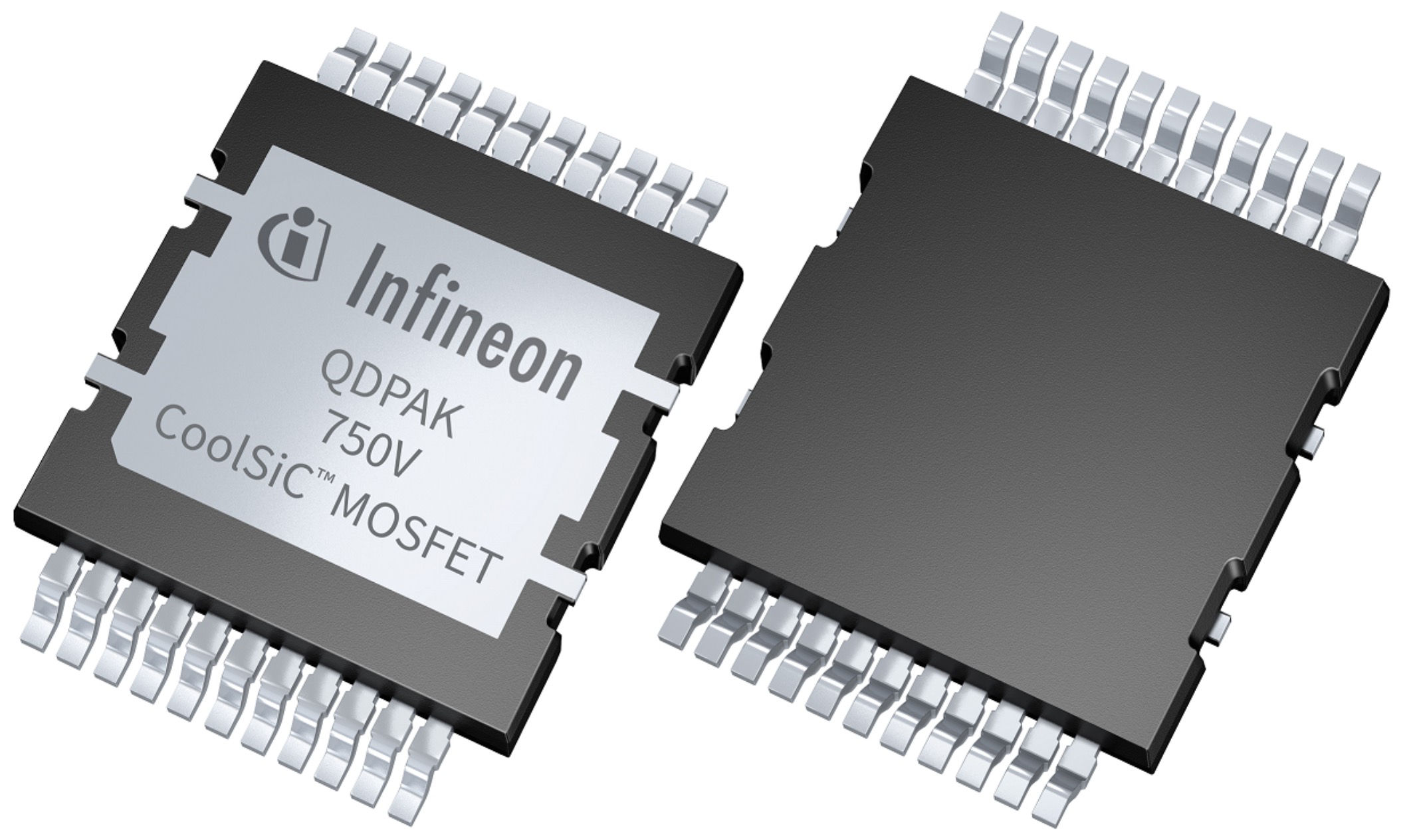
Infineon QDPAK and DDPAK top-side cooling packages registered as JEDEC standard for high-power applications
Technology news
Munich, Germany – 9 February, 2023 – The trends toward higher power density and cost optimization dominate the development goals of efficient high-power applications that create substantial value for segments such as electromobility. To push these boundaries, Infineon Technologies AG (FSE: IFX / OTCQX: IFNNY) today announced it has successfully registered its QDPAK and DDPAK top-side cooling (TSC) packages, which are ideal for high-voltage MOSFETs as a JEDEC standard. This registration further solidifies Infineon’s goal to help establish a broad adoption of TSC in new designs with one standard package design and footprint. Additionally, this provides flexibility and comfort to OEM manufacturers to differentiate their products in the market and take power density to the next level to support various applications.
“As a solutions provider, Infineon continues to influence the semiconductor industry through innovative packaging technologies and manufacturing processes,” said Ralf Otremba, Lead Principal Engineer for High Voltage Packaging, Infineon. “Our advanced top-side cooled packages bring significant advantages to the device and system levels to fulfill the challenging demands of cutting-edge high-power designs. Package outline standardization will help ease one of the main design concerns of OEMs for high-voltage applications by securing pin-to-pin compatibility across vendors.”
For more than 50 years, the JEDEC organization has been the global leader in developing open standards and publications for the microelectronics industry for a broad range of technologies, including package outlines. JEDEC has been widely accepting semiconductor packages such as the TO220 and TO247 through-hole devices (THD) – devices that have been prominently used over the past decades and are still an option in new onboard charger (OBC) designs, high voltage (HV) and low voltage (LV) DC-DC converters.
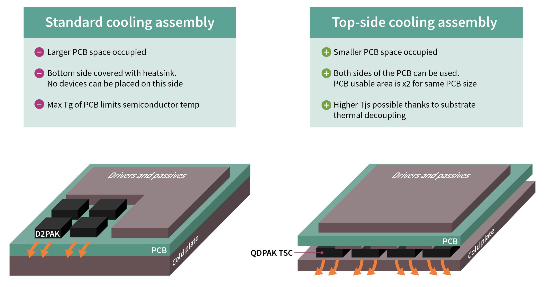
The registration of QDPAK and DDPAK surface-mounted (SMD) TSC package designs signals a new era for package outlines ushering a wide market adoption of the TSC technology as a replacement for TO247 and TO220, respectively. With the benefits of this technology, this new JEDEC package family registration, according to the MO-354 standard, serves as a key enabler for the transition of high-voltage industrial and automotive applications to top-side cooled designs in next-generation platforms.
To facilitate design transition for customers from the TO220 and TO247 THD devices, Infineon has designed QDPAK and DDPAK SMD devices to deliver equivalent thermal capabilities with improved electrical performance. Based on a standard height of 2.3 mm for QDPAK and DDPAK SMD TSC package for HV and LV devices, developers are now able to design complete applications such as OBC and DC-DC conversion with all SMD TSC devices measuring the same height. Compared to existing solutions that require a 3D cooling system, this facilitates designs and reduces system cost for cooling.
Additionally, TSC packaging offers up to 35 percent lower thermal resistance than standard bottom-side cooling (BSC). By enabling the use of both PCB sides, TSC packages offer better board space utilization and at least two times more power density. The thermal management of the packages is also improved by thermal decoupling from the substrate since the thermal resistance of the leads is much higher compared to the exposed package top side. Because of the improved thermal performance, stacking different boards is not necessary. Rather than combining both FR4 and IMS, a single FR4 is enough for all components and also requires fewer connectors. These features deliver an overall bill of materials (BOM), which ultimately reduces overall system cost.
In addition to improved thermal and power capabilities, TSC technology also offers an optimized power loop design for increased reliability. This is possible by the placement of the drivers, which can be placed very close to the power switch. The low stray inductance of the driver switch loop, reduces the loop parasitics and leads to less ringing on the gate, higher performance and a smaller risk of failures.
Additional information is available at www.infineon.com/ddpak and www.infineon.com/obc
More information about Infineon’s contribution to energy efficiency: www.infineon.com/green-energy.
Press Photos

Packaging JEDEC Application
The registration of QDPAK and DDPAK surface-mounted (SMD) TSC package designs signals a new era for package outlines ushering a wide market adoption of the TSC technology as a replacement for TO247 and TO220, respectively.
JPEG
2126x1118 px

Packaging JEDEC Product
The registration of QDPAK and DDPAK surface-mounted (SMD) TSC package designs signals a new era for package outlines ushering a wide market adoption of the TSC technology as a replacement for TO247 and TO220, respectively.
JPEG
2126x1264 px
Share in WeChat
Scan the QR code with your WeChat App to share this page.
Information Number : INFPSS202302-057