- ASIC
- Battery management ICs
- Clocks and timing solutions
- ESD and surge protection devices
- Automotive Ethernet
- Evaluation Boards
- High reliability
- Isolation
- Memories
- Microcontroller
- Power
- RF
- Security and smart card solutions
- Sensor technology
- Small signal transistors and diodes
- Transceivers
- Universal Serial Bus (USB)
- Wireless connectivity
- Search Tools
- Technology
- Packages
- Product Information
- Ordering
- Overview
- Automotive Ethernet PHY for in-vehicle networking
- Automotive Ethernet Switches for in-vehicle networking
- Overview
- Embedded flash IP solutions
- Flash+RAM MCP solutions
- F-RAM (Ferroelectric RAM)
- NOR flash
- nvSRAM (non-volatile SRAM)
- PSRAM – Pseudostatic RAM
- Radiation hardened and high-reliability memories
- SRAM (static RAM)
- Wafer and die memory solutions
- Overview
- AURIX™ TriCore™ MCUs
- PSOC™ MCUs
- TRAVEO™ T2G MCUs
- XMC™ MCUs
- Legacy MCUs
- MOTIX™ motor control SoCs/SIPs
- Overview
- AC-DC power conversion
- Automotive conventional powertrain ICs
- Class D audio amplifier ICs
- Contactless power and sensing ICs
- DC-DC converters
- Diodes and thyristors (Si/SiC)
- eFuses
- Gallium nitride (GaN)
- Gate Driver ICs
- IGBTs – Insulated gate bipolar transistors
- Intelligent power modules (IPM)
- JFETs
- LED driver ICs
- Motor drivers
- MOSFETs
- Power modules
- Power supply ICs
- Protection and monitoring ICs
- Silicon carbide (SiC)
- Smart power switches
- Solid state relays and isolators
- Wireless charging ICs
- Overview
- Antenna cross switches
- Antenna tuners
- Bias and control
- Coupler
- Driver amplifiers
- Rad hard microwave and RF
- Low noise amplifiers (LNAs)
- RF diode
- RF switches
- RF transistors
- Wireless control receiver
- Overview
- Calypso® products
- CIPURSE™ products
- Contactless memories
- OPTIGA™ embedded security solutions
- SECORA™ security solutions
- Security controllers
- Smart card modules
- Smart solutions for government ID
- Overview
- ToF 3D image sensors
- Current sensors
- Gas sensors
- Inductive position sensors
- MEMS microphones
- Pressure sensors
- Radar sensors
- Magnetic position sensors
- Magnetic speed sensors
- Capacitive sensors
- Temperature sensors
- Battery sensors
- Digital X-ray
- Computed tomography
- Sensor interface ASICs
- Overview
- Bipolar transistors
- Diodes
- Small signal/small power MOSFET
- Overview
- Automotive transceivers
- Control communication
- Powerline communications
- Overview
- USB 2.0 peripheral controllers
- USB 3.2 peripheral controllers
- USB hub controllers
- USB PD high-voltage microcontrollers
- USB-C AC-DC and DC-DC charging solutions
- USB-C charging port controllers
- USB-C Power Delivery controllers
- Overview
- AIROC™ Automotive wireless
- AIROC™ Bluetooth® and multiprotocol
- AIROC™ connected MCU
- AIROC™ Wi-Fi + Bluetooth® combos
- AIROC™ Ultra-Wide Band Solutions
- Overview
- Commercial off-the-shelf (COTs) memory portfolio
- Defense memory portfolio
- High-reliability power conversion and management
- Overview
- Rad hard microwave and RF
- Radiation hardened power
- Space memory portfolio
- Overview
- Parallel NOR flash
- SEMPER™ NOR flash family
- SEMPER™ X1 LPDDR flash
- Serial NOR flash
- Overview
-
32-bit TriCore™ AURIX™ – TC2x
- Overview
- AURIX™ family – TC21xL
- AURIX™ family – TC21xSC (wireless charging)
- AURIX™ family – TC22xL
- AURIX™ family – TC23xL
- AURIX™ family – TC23xLA (ADAS)
- AURIX™ family – TC23xLX
- AURIX™ family – TC264DA (ADAS)
- AURIX™ family – TC26xD
- AURIX™ family – TC27xT
- AURIX™ family – TC297TA (ADAS)
- AURIX™ family – TC29xT
- AURIX™ family – TC29xTT (ADAS)
- AURIX™ family – TC29xTX
- AURIX™ TC2x emulation devices
-
32-bit TriCore™ AURIX™ – TC3x
- Overview
- AURIX™ family - TC32xLP
- AURIX™ family – TC33xDA
- AURIX™ family - TC33xLP
- AURIX™ family – TC35xTA (ADAS)
- AURIX™ family – TC36xDP
- AURIX™ family – TC37xTP
- AURIX™ family – TC37xTX
- AURIX™ family – TC38xQP
- AURIX™ family – TC39xXA (ADAS)
- TC39xXX/XP
- AURIX™ family – TC3Ex
- AURIX™ TC37xTE (emulation devices)
- AURIX™ TC39xXE (emulation devices)
- 32-bit TriCore™ AURIX™ – TC4x
- Overview
- PSOC™ 4 Arm® Cortex®-M0/M0+
- PSOC™ 4 HV Arm® Cortex®-M0+
- PSOC™ 5 LP Arm® Cortex®-M3
- PSOC™ 6 Arm® Cortex®-M4/M0+
- PSOC™ Multitouch Touchscreen Controller
- PSOC™ Control C3 Arm® Cortex®-M33
- PSOC™ Automotive 4: Arm® Cortex®-M0/M0+
- PSOC™ Edge Arm® Cortex® M55/M33
- PSOC™ Control C1 Arm® Cortex®-M0
- Overview
- 32-bit TRAVEO™ T2G Arm® Cortex® for body
- 32-bit TRAVEO™ T2G Arm® Cortex® for cluster
- Overview
- 32-bit XMC1000 industrial microcontroller Arm® Cortex®-M0
- 32-bit XMC4000 industrial microcontroller Arm® Cortex®-M4
- XMC5000 Industrial Microcontroller Arm® Cortex®-M4F
- 32-bit XMC7000 Industrial Microcontroller Arm® Cortex®-M7
- Overview
- Legacy 32-bit MCU
- Legacy 8-bit/16-bit microcontroller
- Other legacy MCUs
- 32-bit FM Arm® Cortex® Microcontroller
- Sensing controllers
- Overview
- AC-DC integrated power stage - CoolSET™
- AC-DC PWM and PFC controller
- Overview
- Bridge rectifiers & AC switches
- CoolSiC™ Schottky diodes
- Diode bare dies
- Silicon diodes
- Thyristor / Diode Power Modules
- Thyristor soft starter modules
- Thyristor/diode discs
- Overview
- GaN bidirectional switches
- GaN smart
- GaN transistors (GaN HEMTs)
- GaN with integrated driver
- GaN bare dies
- Overview
- Automotive gate driver ICs
- Gate Driver ICs for GaN HEMTs
- Gate Driver ICs for SiC MOSFETs
- Half-Bridge Gate Driver ICs
- High-Side Gate Driver ICs
- Isolated Gate Driver ICs
- Level-Shift Gate Driver ICs
- Low-Side Gate Driver ICs
- Three-Phase Gate Driver ICs
- Transformer Driver ICs
- Overview
- AC-DC LED driver ICs
- Ballast IC
- DC-DC LED driver IC
- LED dimming interface IC
- Linear LED driver IC
- LITIX™ - Automotive LED Driver IC
- NFC wireless configuration IC with PWM output
- VCSEL driver
- Overview
- BLDC motor drivers
- BDC motor drivers
- Stepper & servo motor drivers
- Motor drivers with MCU
- Bridge drivers with MOSFETs
- Gate Driver ICs
- Overview
- Automotive MOSFET
- Dual MOSFETs
- MOSFET (Si & SiC) Modules
- N-channel depletion mode MOSFET
- N-channel MOSFETs
- P-channel MOSFETs
-
Silicon carbide CoolSiC™ MOSFETs
- Overview
- Silicon Carbide MOSFET modules
- Silicon carbide MOSFET discretes
- Silicon carbide MOSFETs bare dies
- 400 V / 440 V Silicon Carbide MOSFETs
- 650 V Silicon Carbide MOSFETs
- 750 V Silicon Carbide MOSFETs
- 1200 V Silicon Carbide MOSFETs
- 2000 V Silicon Carbide MOSFETs
- 2300 V Silicon Carbide MOSFETs
- 3300 V Silicon Carbide MOSFETs
- 1700 V Silicon Carbide MOSFETs
- Small signal/small power MOSFET
- Overview
- IGBT modules
- MOSFET (Si & SiC) Modules
- Intelligent power modules (IPM)
- Diodes and thyristors (Si/SiC)
- Automotive IGBT and CoolSiC™ MOSFET modules
- High density power modules
- Overview
- Automotive transceivers
- Linear voltage regulators for automotive applications
- OPTIREG™ PMIC
- OPTIREG™ switcher
- OPTIREG™ System Basis Chips (SBC)
- Overview
- High-side switches
- Low-side switches
- Multichannel SPI Switches & Controller
- Automotive eFuses
- Overview
- Radar sensors for automotive
- Radar sensors for IoT
- Overview
- EZ-USB™ CX3 MIPI CSI2 to USB 3.0 camera controller
- EZ-USB™ FX10 & FX5N USB 10Gbps peripheral controller
- EZ-USB™ FX20 USB 20 Gbps peripheral controller
- EZ-USB™ FX3 USB 5 Gbps peripheral controller
- EZ-USB™ FX3S USB 5 Gbps peripheral controller with storage interface
- EZ-USB™ FX5 USB 5 Gbps peripheral controller
- EZ-USB™ SD3 USB 5 Gbps storage controller
- EZ-USB™ SX3 FIFO to USB 5 Gbps peripheral controller
- Overview
- EZ-PD™ PMG1-B1 Battery Charge Controller with USB-C PD MCU
- EZ-PD™ PMG1-S0 high-voltage MCU with USB-C and PD
- EZ-PD™ PMG1-S1 high-voltage MCU with USB-C and PD
- EZ-PD™ PMG1-S2 high-voltage MCU with USB PD
- EZ-PD™ PMG1-S3 high-voltage MCU with USB-C & PD
- EZ-PD™ PMG1-B2 Battery Charge Controller with USB-C PD MCU
- Overview
- EZ-PD™ CCG3 USB type-C port controller PD
- EZ-PD™ CCG3PA USB-C and PD
- EZ-PD™ CCG3PA-NFET USB-C PD controller
- EZ-PD™ CCG7x consumer USB-C Power Delivery & DC-DC controller
- EZ-PD™ PAG1: power adapter generation 1
- EZ-PD™ PAG2: Power Adapter Generation 2
- EZ-PD™ PAG2-PD USB-C PD Controller
- Overview
- EZ-PD™ ACG1F one-port USB-C controller
- EZ-PD™ CCG2 USB Type-C port controller
- EZ-PD™ CCG3PA Automotive USB-C and Power Delivery controller
- EZ-PD™ CCG4 two-port USB-C and PD
- EZ-PD™ CCG5 dual-port and CCG5C single-port USB-C PD controllers
- EZ-PD™ CCG6 one-port USB-C & PD controller
- EZ-PD™ CCG6_CFP and EZ-PD™ CCG8_CFP Dual-Single-Port USB-C PD
- EZ-PD™ CCG6DF dual-port and CCG6SF single-port USB-C PD controllers
- EZ-PD™ CCG7D Automotive dual-port USB-C PD + DC-DC controller
- EZ-PD™ CCG7S Automotive single-port USB-C PD solution with a DC-DC controller + FETs
- EZ-PD™ CCG8 dual-single-port USB-C PD
- EZ-PD™ CMG1 USB-C EMCA controller
- EZ-PD™ CMG2 USB-C EMCA controller with EPR
Browse by core architecture
Browse by key technologies
- LATEST IN
- Aerospace and defense
- AI and data center
- Automotive
- Communications
- Consumer electronics
- Health and lifestyle
- Industrial
- Security solutions
- Smart home and building
- Solutions
- Overview
- Defense applications
- Space applications
- Overview
- Data center power solutions
- Edge computing
- Machine Learning Edge AI
- Overview
- ADAS & autonomous driving
- Automotive body electronics
- Automotive LED lighting systems
- Automotive zonal architecture
- Chassis control & safety
- Electric vehicle drivetrain system
- EV thermal management system
- In-vehicle infotainment & HMI
- Light electric vehicle solutions
- Overview
- Satellite communications
- Telecommunications infrastructure
- Overview
- Power adapters and chargers
- Complete system solutions for smart TVs
- Mobile device and smartphone solutions
- Semiconductor solutions for home entertainment applications
- Smart conference systems
- Drones
- AR and smart glasses
- Photovoltaic
- Consumer Wearables
- Home appliances
- Overview
- Power adapters and chargers
- Asset Tracking
- Battery formation and testing
- Electric forklifts
- Battery energy storage (BESS)
- EV charging
- High voltage solid-state power distribution
- Industrial automation
- Industrial motor drives and controls
- Industrial robots
- LED lighting system design
- Light electric vehicle solutions
- Power transmission and distribution
- Traction
- Uninterruptible power supplies (UPS)
- Digital health
- Robotics
- Wind power
- Hydrogen electrolysis
- Photovoltaic
- Industrial & Medical SMPS
- Power tools
- Overview
- Device authentication and brand protection
- Embedded security for the Internet of Things (IoT)
- eSIM applications
- Government identification
- Mobile security
- Payment solutions
- Access control and ticketing
- Overview
- Domestic robots
- Heating ventilation and air conditioning (HVAC)
- Home and building automation
- PC accessories
- Semiconductor solutions for home entertainment applications
- Overview
- Battery management systems (BMS)
- Connectivity
- Human Machine Interface
- Machine Learning Edge AI
- Motor control
- Power conversion
- Security
- Sensor solutions
- System diagnostics and analytics
- Overview
- FPGAs in datacenter applications
- Power system reliability modeling
-
Server rack power management
- Overview
- Server power supply units (PSU)
- Server battery backup units (BBU)
- Intermediate Bus Converter (IBC)
- Ampere CPU voltage regulator Ics
- Intel CPU voltage regulator Ics
- AMD CPU voltage regulator Ics
- AI accelerator cards
- SmartNIC cards
- Network switches for AI data centers and server racks
- Server power path protection
- Data center power distribution
- Overview
- Automotive animated LED lighting system
- Automotive LED front single light functions
- Automotive LED rear single light functions
- Full LED headlight system - multi-channel LED driver
- LED drivers (electric two- & three-wheelers)
- LED pixel light controller - supply & communication
- Static interior ambient LED light
- Overview
- Active suspension control
- Automotive braking solutions
- Automotive steering solutions
- Chassis domain control
- Overview
-
Automotive BMS
- Overview
- Automotive battery cell monitoring & balancing
- Automotive battery control unit (BCU)
- Automotive battery isolated communication
- Automotive battery management system (BMS) - 12 V to 24 V
- Automotive battery management system (BMS) - 48 V
- Automotive battery management system (BMS) - high-voltage
- Automotive battery pack monitoring
- Automotive battery passport & event logging
- Automotive battery protection & disconnection
- Automotive current sensing & coulomb counting
- BMS (electric two- & three-wheelers)
- EV charging
- FCEV powertrain system
- Auxiliary inverter
- Auxiliary inverter - high-voltage (commercial vehicles)
- EV traction inverter
- Traction inverter (electric commercial vehicles)
- Traction inverter (electric two- & three-wheelers)
- DC-DC converter high-voltage
- DC-DC converter high-voltage (commercial vehicles)
- On-board charging (electric commercial vehicles)
- On-board charging (OBC)
- On-board charging (OBC) solutions for electric two- and three-wheelers
- Overview
- AC-DC power conversion for telecommunications infrastructure
- DC-DC power conversion for telecommunications infrastructure
- FPGA in wired and wireless telecommunications applications
- Power system reliability modeling
- RF front end components for telecommunications infrastructure
- Memory solutions for cellular base stations
- Security solutions for cellular base stations
- Overview
- Audio amplifier solutions
- Complete system solutions for smart TVs
- Distribution audio amplifier unit solutions
- Home theater installation speaker system solutions
- Party speaker solutions
- PoE audio amplifier unit solutions
- Portable speaker solutions
- Powered active speaker systems
- Remote control
- Smart speaker designs
- Soundbar solutions
- Overview
- Data center power solutions
- Digital input/output (I/O) modules
- DIN rail power supply solutions
- Home and building automation
- Industrial HMI Monitors and Panels
- Industrial motor drives and controls
- Industrial PC
- Industrial robots
- Machine vision
- Mobile robots (AGV, AMR)
- Programmable logic controller (PLC)
- Solid-state circuit breaker (SSCB)
- Uninterruptible power supplies (UPS)
- Overview
- Durable healthcare equipment
- Disposable healthcare equipment
- Healthcare wearables
- Overview
- Automotive BMS
- Industrial and consumer BMS
- Overview
- AC-DC power conversion
- DC-DC power conversion
- Overview
- Power supply health monitoring
- LATEST IN
- Digital documentation
- Boards & Kits
- Finder & selection tools
- Platforms
- Services
- Simulation & Modeling
- Software
- Tools
- Partners
- Infineon for Makers
- University Alliance Program
- Overview
- Bipolar Discs Finder
- Bipolar Module Finder
- Connected Secure Systems Finder
- Diode Rectifier Finder
- ESD Protection Finder
- Evaluation Board Finder
- Gate Driver Finder
- IGBT Discrete Finder
- IGBT Module Finder
- IPM Finder
- Microcontroller Finder
- MOSFET Finder
- PMIC Finder
- Product Finder
- PSOC™ and FMx MCU Board & Kit Finder
- Radar Finder
- Reference Design Finder
- Simulation Model Finder
- Smart Power Switch Finder
- Transceiver Finder
- Voltage Regulator Finder
- Wireless Connectivity Board & Kit Finder
- Overview
- AIROC™ software & tools
- AURIX™ software & tools
- DRIVECORE™ for automotive software development
- iMOTION™ software & tools
- Infineon Smart Power Switches & Gate Driver Tool Suite
- MOTIX™ software & tools
- OPTIGA™ software & tools
- PSOC™ software & tools
- TRAVEO™ software & tools
- XENSIV™ software & tools
- XMC™ software & tools
- Overview
- CoolGaN™ Simulation Tool (PLECS)
- HiRel Fit Rate Tool
- Infineon Designer
- Interactive product sheet
- IPOSIM Online Power Simulation Platform
- InfineonSpice Offline Simulation Tool
- OPTIREG™ automotive power supply ICs Simulation Tool (PLECS)
- Power MOSFET Simulation Models
- PowerEsim Switch Mode Power Supply Design Tool
- Solution Finder
- XENSIV™ Magnetic Sensor Simulation Tool
- Overview
- AURIX™ certifications
- AURIX™ development tools
-
AURIX™ Embedded Software
- Overview
- AURIX™ Applications software
- AURIX™ Artificial Intelligence
- AURIX™ Gateway
- AURIX™ iLLD Drivers
- Infineon safety
- AURIX™ Security
- AURIX™ TC3xx Motor Control Application Kit
- AURIX™ TC4x SW application architecture
- Infineon AUTOSAR
- Communication and Connectivity
- Middleware
- Non AUTOSAR OS/RTOS
- OTA
- AURIX™ Microcontroller Kits
- Overview
- TRAVEO™ Development Tools
- TRAVEO™ Embedded Software
- Overview
- XENSIV™ Development Tools
- XENSIV™ Embedded Software
- XENSIV™ evaluation boards
- Overview
- CAPSENSE™ Controllers Code Examples
- Memories for Embedded Systems Code Examples
- PSOC™ 1 Code Examples for PSOC™ Designer
- PSOC™ 3 Code Examples for PSOC™ Creator
- PSOC™ 3/4/5 Code Examples
- PSOC™ 4 Code Examples for PSOC™ Creator
- PSOC™ 6 Code Examples for PSOC™ Creator
- PSOC™ 63 Code Examples
- USB Controllers Code Examples
- Overview
- DEEPCRAFT™ AI Hub
- DEEPCRAFT™ Audio Enhancement
- DEEPCRAFT™ Model Converter
-
DEEPCRAFT™ Ready Models
- Overview
- DEEPCRAFT™ Ready Model for Baby Cry Detection
- DEEPCRAFT™ Ready Model for Cough Detection
- DEEPCRAFT™ Ready Model for Direction of Arrival (Sound)
- DEEPCRAFT™ Ready Model for Factory Alarm Detection
- DEEPCRAFT™ Ready Model for Fall Detection
- DEEPCRAFT™ Ready Model for Gesture Classification
- DEEPCRAFT™ Ready Model for Siren Detection
- DEEPCRAFT™ Ready Model for Snore Detection
- DEEPCRAFT™ Studio
- DEEPCRAFT™ Voice Assistant
- Overview
- AIROC™ Wi-Fi & Bluetooth EZ-Serial Module Firmware Platform
- AIROC™ Wi-Fi & Bluetooth Linux and Android Drivers
- emWin Graphics Library and GUI for PSOC™
- Infineon Complex Device Driver for Battery Management Systems
- Memory Solutions Hub
- PSOC™ 6 Peripheral Driver Library (PDL) for PSOC™ Creator
- USB Controllers EZ-USB™ GX3 Software and Drivers
- Overview
- CAPSENSE™ Controllers Configuration Tools EZ-Click
- DC-DC Integrated POL Voltage Regulators Configuration Tool – PowIRCenter
- EZ-USB™ SX3 Configuration Utility
- FM+ Configuration Tools
- FMx Configuration Tools
- Tranceiver IC Configuration Tool
- USB EZ-PD™ Configuration Utility
- USB EZ-PD™ Dock Configuration Utility
- USB EZ-USB™ HX3C Blaster Plus Configuration Utility
- USB UART Config Utility
- XENSIV™ Tire Pressure Sensor Programming
- Overview
- EZ-PD™ CCGx Dock Software Development Kit
-
FMx Softune IDE
- Overview
- RealOS™ Real-Time Operating System
- Softune IDE Language tools
- Softune Workbench
- Tool Lineup for F2MC-16 Family SOFTUNE V3
- Tool Lineup for F2MC-8FX Family SOFTUNE V3
- Tool Lineup for FR Family SOFTUNE V6
- Virtual Starter Kit
- Windows 10 operation of released SOFTUNE product
- Windows 7 operation of released SOFTUNE product
- Windows 8 operation of released SOFTUNE product
- ModusToolbox™ Software
- PSOC™ Creator Software
- Radar Development Kit
- RUST
- USB Controllers SDK
- Wireless Connectivity Bluetooth Mesh Helper Applications
- XMC™ DAVE™ Software
- Overview
- AIROC™ Bluetooth® Connect App Archive
- Cypress™ Programmer Archive
- EZ-PD™ CCGx Power Software Development Kit Archive
- ModusToolbox™ Software Archive
- PSOC™ Creator Archive
- PSOC™ Designer Archive
- PSOC™ Programmer Archive
- USB EZ-PD™ Configuration Utility Archives
- USB EZ-PD™ Host SDK Archives
- USB EZ-USB™ FX3 Archive
- USB EZ-USB™ HX3PD Configuration Utility Archive
- WICED™ Smart SDK Archive
- WICED™ Studio Archive
- Overview
- Infineon Developer Center Launcher
- Infineon Register Viewer
- Pin and Code Wizard
- Timing Solutions
- Wireless Connectivity
- LATEST IN
- Support
- Training
- Developer Community
- News
Business & Financial Press
Jul 13, 2026
Business & Financial Press
Jul 07, 2026
Business & Financial Press
Jul 03, 2026
Business & Financial Press
Jul 02, 2026
- Company
- Our stories
- Events
- Press
- Investor
- Careers
- Quality
- Latest news
Business & Financial Press
Jul 13, 2026
Business & Financial Press
Jul 07, 2026
Business & Financial Press
Jul 03, 2026
Business & Financial Press
Jul 02, 2026
Product details
-
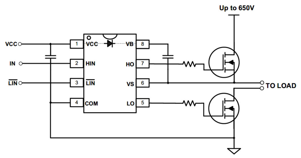
Channels2
-
ConfigurationHalf-Bridge
-
Input Vcc range10 V to 20 V
-
Isolation TypeFunctional levelshift SOI (Silicon On Insulator)
-
Output Current (Source)0.29 A
-
Output Current (Sink)0.7 A
-
PackagePG-DSO-8
-
Product Name2ED2103S06F
-
QualificationIndustrial
-
Turn Off Propagation Delay90 ns
-
Turn On Propagation Delay90 ns
-
VBS UVLO (On)8.9 V
-
VBS UVLO (Off)8 V
-
VCC UVLO (Off)8 V
-
VCC UVLO (On)8.9 V
-
Voltage Class650 V
| Recommended | ||
|
OPN
|
2ED2103S06FXUMA1 | |
| Product Status | active and preferred | |
| Infineon Package | ||
| Package Name | N/A | |
| Packing Size | 2500 | |
| Packing Type | TAPE & REEL | |
| Moisture Level | 2 | |
| Moisture Packing | DRY | |
| Lead-free | Yes | |
| Halogen Free | Yes | |
| RoHS Compliant | Yes | |
|
Infineon stock last updated:
|
ea.
in stock
|
|
|
|
||
|
|
||
| Product Status |
Active
|
|---|---|
| Infineon Package | |
| Package Name | - |
| Packing Size | 2500 |
| Packing Type | TAPE & REEL |
| Moisture Level | 2 |
| Moisture Packing | DRY |
| Lead Free | |
| Halogen Free | |
| RoHS Compliant | |
Features
- Op. voltages (VS node) < + 650 V
- Neg. VS transient immunity of 100 V
- Integr. ultra-fast bootstrap diode
- 90 ns propagation delay
- Cross-conduction prevention logic
- Internal 520 ns dead time
- HIN, /LIN logic input
- Floating channel for bootstrap op.
- Independent UVLO for both channels
- Logic op. up to –11 V on VS Pin
- Neg. voltage tol. on inputs of –5 V
- Maximum supply voltage of 25 V
Diagrams
Share in WeChat
Scan the QR code with your WeChat App to share this page.