- ASIC
- Battery management ICs
- Clocks and timing solutions
- ESD and surge protection devices
- Automotive Ethernet
- Evaluation Boards
- High reliability
- Isolation
- Memories
- Microcontroller
- Power
- RF
- Security and smart card solutions
- Sensor technology
- Small signal transistors and diodes
- Transceivers
- Universal Serial Bus (USB)
- Wireless connectivity
- Search Tools
- Technology
- Packages
- Product Information
- Where to Buy
- Overview
- Automotive Ethernet Bridges
- Automotive Ethernet PHY for in-vehicle networking
- Automotive Ethernet Switches for in-vehicle networking
- Overview
- Defense
- High-reliability custom services
- NewSpace
- Space
- Overview
- Embedded flash IP solutions
- Flash+RAM MCP solutions
- F-RAM (Ferroelectric RAM)
- NOR flash
- nvSRAM (non-volatile SRAM)
- PSRAM (Pseudostatic RAM)
- Radiation hardened and high-reliability memories
- RRAM Resistive Ram
- SRAM (static RAM)
- Wafer and die memory solutions
- Overview
- 32-bit FM Arm® Cortex® Microcontroller
- 32-bit AURIX™ TriCore™ microcontroller
- 32-bit PSOC™ Arm® Cortex® microcontroller
- 32-bit TRAVEO™ T2G Arm® Cortex® microcontroller
- 32-bit XMC™ industrial microcontroller Arm® Cortex®-M
- Legacy microcontroller
- MOTIX™ MCU | 32-bit motor control SoC based on Arm® Cortex®-M
- Sensing controllers
- Overview
- AC-DC power conversion
- Automotive conventional powertrain ICs
- Class D audio amplifier ICs
- Contactless power and sensing ICs
- DC-DC converters
- Diodes and thyristors (Si/SiC)
- Gallium nitride (GaN)
- Gate driver ICs
- IGBTs – Insulated gate bipolar transistors
- Intelligent power modules (IPM)
- LED driver ICs
- Motor control ICs
- Power MOSFETs
- Power modules
- Power supply ICs
- Protection and monitoring ICs
- Silicon carbide (SiC)
- Smart power switches
- Solid state relays
- Wireless charging ICs
- Overview
- Antenna cross switches
- Antenna tuners
- Bias and control
- Coupler
- Driver amplifiers
- High Reliability Discrete
- Low noise amplifiers (LNAs)
- RF diode
- RF switches
- RF transistors
- Wireless control receiver
- Overview
- Calypso® products
- CIPURSE™ products
- Contactless memories
- OPTIGA™ embedded security solutions
- SECORA™ security solutions
- Security controllers
- Smart card modules
- Smart solutions for government ID
- Overview
- ToF 3D image sensors
- Current sensors
- Gas sensors
- Inductive position sensors
- MEMS microphones
- Pressure sensors
- Radar sensors
- Magnetic position sensors
- Magnetic speed sensors
- Overview
- Bipolar transistors
- Diodes
- Small signal/small power MOSFET
- Overview
- Automotive transceivers
- Control communication
- Powerline communications
- Overview
- USB 2.0 peripheral controllers
- USB 3.2 peripheral controllers
- USB hub controllers
- USB PD high-voltage microcontrollers
- USB-C AC-DC and DC-DC charging solutions
- USB-C charging port controllers
- USB-C Power Delivery controllers
- Overview
- AIROC™ Automotive wireless
- AIROC™ Bluetooth® and multiprotocol
- AIROC™ connected MCU
- AIROC™ Wi-Fi + Bluetooth® combos
- Overview
- Commercial off-the-shelf (COTs) memory portfolio
- Defense memory portfolio
- High-reliability power conversion and management
- Overview
- Rad hard microwave and RF
- Radiation hardened power
- Space memory portfolio
- Overview
- Parallel NOR flash
- SEMPER™ NOR flash family
- SEMPER™ X1 LPDDR flash
- Serial NOR flash
- Overview
- FM0+ 32-bit Arm® Cortex®-M0+ microcontroller (MCU) families
-
FM3 32-bit Arm® Cortex®-M3 microcontroller (MCU) families
- Overview
- FM3 CY9AFx1xK series Arm® Cortex®-M3 microcontroller (MCU)
- FM3 CY9AFx1xL/M/N series Arm® Cortex®-M3 microcontroller (MCU)
- FM3 CY9AFx2xK/L series Arm® Cortex®-M3 microcontroller (MCU)
- FM3 CY9AFx3xK/L series ultra-low leak Arm® Cortex®-M3 microcontroller (MCU)
- FM3 CY9AFx4xL/M/N series low power Arm® Cortex®-M3 microcontroller (MCU)
- FM3 CY9AFx5xM/N/R series low power Arm® Cortex®-M3 microcontroller (MCU)
- FM3 CY9AFxAxL/M/N series ultra-low leak Arm® Cortex®-M3 microcontroller (MCU)
- FM3 CY9BFx1xN/R high-performance series Arm® Cortex®-M3 microcontroller (MCU)
- FM3 CY9BFx1xS/T high-performance series Arm® Cortex®-M3 microcontroller (MCU)
- FM3 CY9BFx2xJ series Arm® Cortex®-M3 microcontroller (MCU)
- FM3 CY9BFx2xK/L/M series Arm® Cortex®-M3 microcontroller (MCU)
- FM3 CY9BFx2xS/T series Arm® Cortex®-M3 microcontroller (MCU)
-
FM4 32-bit Arm® Cortex®-M4 microcontroller (MCU) families
- Overview
- FM4 CY9BFx6xK/L high-performance series Arm® Cortex®-M4F microcontroller (MCU)
- FM4 CY9BFx6xM/N/R high-performance series Arm® Cortex®-M4F microcontroller (MCU)
- FM4 S6E2C high-performance series Arm® Cortex®-M4F microcontroller (MCU)
- FM4 S6E2G series connectivity Arm® Cortex®-M4F microcontroller (MCU)
- FM4 S6E2H high-performance series Arm® Cortex®-M4F microcontroller (MCU)
- Overview
-
32-bit TriCore™ AURIX™ – TC2x
- Overview
- AURIX™ family – TC21xL
- AURIX™ family – TC21xSC (wireless charging)
- AURIX™ family – TC22xL
- AURIX™ family – TC23xL
- AURIX™ family – TC23xLA (ADAS)
- AURIX™ family – TC23xLX
- AURIX™ family – TC264DA (ADAS)
- AURIX™ family – TC26xD
- AURIX™ family – TC27xT
- AURIX™ family – TC297TA (ADAS)
- AURIX™ family – TC29xT
- AURIX™ family – TC29xTT (ADAS)
- AURIX™ family – TC29xTX
- AURIX™ TC2x emulation devices
-
32-bit TriCore™ AURIX™ – TC3x
- Overview
- AURIX™ family - TC32xLP
- AURIX™ family – TC33xDA
- AURIX™ family - TC33xLP
- AURIX™ family – TC35xTA (ADAS)
- AURIX™ family – TC36xDP
- AURIX™ family – TC37xTP
- AURIX™ family – TC37xTX
- AURIX™ family – TC38xQP
- AURIX™ family – TC39xXA (ADAS)
- AURIX™ family – TC39xXX
- AURIX™ family – TC3Ex
- AURIX™ TC37xTE (emulation devices)
- AURIX™ TC39xXE (emulation devices)
- 32-bit TriCore™ AURIX™ – TC4x
- Overview
- PSOC™ 4 Arm® Cortex®-M0/M0+
- PSOC™ 4 HV Arm® Cortex®-M0+
- PSOC™ 5 LP Arm® Cortex®-M3
- PSOC™ 6 Arm® Cortex®-M4/M0+
- PSOC™ Multitouch Arm® Cortex®-M0
- PSOC™ Control Arm® Cortex®-M33
- PSOC™ Fingerprint Arm® Cortex®-M0+
- PSOC™ Automotive 4: Arm® Cortex®-M0/M0+
- PSOC™ Edge Arm® Cortex® M55/M33
- Overview
- 32-bit TRAVEO™ T2G Arm® Cortex® for body
- 32-bit TRAVEO™ T2G Arm® Cortex® for cluster
- Overview
- 32-bit XMC1000 industrial microcontroller Arm® Cortex®-M0
- 32-bit XMC4000 industrial microcontroller Arm® Cortex®-M4
- XMC5000 Industrial Microcontroller Arm® Cortex®-M4F
- 32-bit XMC7000 Industrial Microcontroller Arm® Cortex®-M7
- Overview
- Legacy 32-bit MCU
- Legacy 8-bit/16-bit microcontroller
- Other legacy MCUs
- Overview
- AC-DC integrated power stage - CoolSET™
- AC-DC PWM-PFC controller
- Overview
- Bridge rectifiers & AC switches
- CoolSiC™ Schottky diodes
- Diode bare dies
- Silicon diodes
- Thyristor / Diode Power Modules
- Thyristor soft starter modules
- Thyristor/diode discs
- Overview
- Automotive gate driver ICs
- Isolated Gate Driver ICs
- Level-Shift Gate Driver ICs
- Low-Side Drivers
- Transformer Driver ICs
- Overview
- AC-DC LED driver ICs
- Ballast IC
- DC-DC LED driver IC
- LED dimming interface IC
- Linear LED driver IC
- LITIX™ - Automotive LED Driver IC
- NFC wireless configuration IC with PWM output
- VCSEL driver
- Overview
- 32-bit PSOC™ Control Arm® Cortex®-M33 MCU
- iMOTION™ Integrated motor control solutions
- MOTIX™ MCU | 32-bit motor control SoC based on Arm® Cortex®-M
- MOTIX™ motor control ICs for BLDC motors
- MOTIX™ motor control ICs for brushed DC motors
- MOTIX™ multi half-bridge ICs for servo and stepper motors
- Overview
- Automotive MOSFET
- Dual MOSFETs
- MOSFET (Si & SiC) Modules
- N-channel depletion mode MOSFET
- N-channel power MOSFETs
- P-channel power MOSFETs
- Silicon carbide CoolSiC™ MOSFETs
- Small signal/small power MOSFET
- Overview
- Automotive transceivers
- Linear Voltage Regulators for Automotive Applications
- OPTIREG™ PMIC
- OPTIREG™ switcher
- OPTIREG™ System Basis Chips (SBC)
- Overview
- eFuse
-
High-side switches
- Overview
- Classic PROFET™ 12V | Automotive smart high-side switch
- Classic PROFET™ 24V | Automotive smart high-side switch
- Power PROFET™ + 12/24/48V | Automotive smart high-side switch
- PROFET™ + 12V | Automotive smart high-side switch
- PROFET™ + 24V | Automotive smart high-side switch
- PROFET™ + 48V | Automotive smart high-side switch
- PROFET™ +2 12V | Automotive smart high-side switch
- PROFET™ Industrial | Smart high-side switch
- PROFET™ Load Guard 12V | Automotive smart high-side switch
- PROFET™ Wire Guard 12V | Automotive eFuse
- Low-side switches
- Multichannel SPI Switches & Controller
- Overview
- Radar sensors for automotive
- Radar sensors for IoT
- Overview
- EZ-USB™ CX3 MIPI CSI2 to USB 3.0 camera controller
- EZ-USB™ FX10 & FX5N USB 10Gbps peripheral controller
- EZ-USB™ FX20 USB 20 Gbps peripheral controller
- EZ-USB™ FX3 USB 5 Gbps peripheral controller
- EZ-USB™ FX3S USB 5 Gbps peripheral controller with storage interface
- EZ-USB™ FX5 USB 5 Gbps peripheral controller
- EZ-USB™ SD3 USB 5 Gbps storage controller
- EZ-USB™ SX3 FIFO to USB 5 Gbps peripheral controller
- Overview
- EZ-PD™ CCG3 USB type-C port controller PD
- EZ-PD™ CCG3PA USB-C and PD
- EZ-PD™ CCG3PA-NFET USB-C PD controller
- EZ-PD™ CCG7x consumer USB-C Power Delivery & DC-DC controller
- EZ-PD™ PAG1: power adapter generation 1
- EZ-PD™ PAG2: Power Adapter Generation 2
- EZ-PD™ PAG2-PD USB-C PD Controller
- Overview
- EZ-PD™ ACG1F one-port USB-C controller
- EZ-PD™ CCG2 USB Type-C port controller
- EZ-PD™ CCG3PA Automotive USB-C and Power Delivery controller
- EZ-PD™ CCG4 two-port USB-C and PD
- EZ-PD™ CCG5 dual-port and CCG5C single-port USB-C PD controllers
- EZ-PD™ CCG6 one-port USB-C & PD controller
- EZ-PD™ CCG6_CFP and EZ-PD™ CCG8_CFP Dual-Single-Port USB-C PD
- EZ-PD™ CCG6DF dual-port and CCG6SF single-port USB-C PD controllers
- EZ-PD™ CCG7D Automotive dual-port USB-C PD + DC-DC controller
- EZ-PD™ CCG7S Automotive single-port USB-C PD solution with a DC-DC controller
- EZ-PD™ CCG7SAF Automotive Single-port USB-C PD + DC-DC Controller + FETs
- EZ-PD™ CCG8 dual-single-port USB-C PD
- EZ-PD™ CMG1 USB-C EMCA controller
- EZ-PD™ CMG2 USB-C EMCA controller with EPR
- LATEST IN
- Aerospace and defense
- Automotive
- Consumer electronics
- Health and lifestyle
- Home appliances
- Industrial
- Information and Communication Technology
- Renewables
- Robotics
- Security solutions
- Smart home and building
- Solutions
- Overview
- Defense applications
- Space applications
- Overview
- 48 V systems for EVs & mild hybrids
- ADAS & autonomous driving
- Automotive body electronics & power distribution
- Automotive LED lighting systems
- Chassis control & safety
- Electric vehicle drivetrain system
- EV thermal management system
- Internal combustion drivetrain systems
- In-vehicle infotainment & HMI
- Light electric vehicle solutions
- Overview
- Adapters and chargers
- Complete system solutions for smart TVs
- Mobile device and smartphone solutions
- Multicopters and drones
- Power tools
- Semiconductor solutions for home entertainment applications
- Smart conference systems
- Overview
- Adapters and chargers
- Asset Tracking
- Battery formation and testing
- Electric forklifts
- Battery energy storage (BESS)
- EV charging
- High voltage solid-state power distribution
- Industrial automation
- Industrial motor drives and controls
- Industrial robots system solutions for Industry 4.0
- LED lighting system design
- Light electric vehicle solutions
- Power tools
- Power transmission and distribution
- Traction
- Uninterruptible power supplies (UPS)
- Overview
- Data center and AI data center solutions
- Edge computing
- Telecommunications infrastructure
- Machine Learning Edge AI
- Overview
- Battery formation and testing
- EV charging
- Hydrogen
- Photovoltaic
- Wind power
- Solid-state circuit breaker
- Battery energy storage (BESS)
- Overview
- Device authentication and brand protection
- Embedded security for the Internet of Things (IoT)
- eSIM applications
- Government identification
- Mobile security
- Payment solutions
- Access control and ticketing
- Overview
- Domestic robots
- Heating ventilation and air conditioning (HVAC)
- Home and building automation
- PC accessories
- Semiconductor solutions for home entertainment applications
- Overview
- Battery management systems (BMS)
- Connectivity
- Human Machine Interface
- Machine Learning Edge AI
- Motor control
- Power conversion
- Security
- Sensor solutions
- System diagnostics and analytics
- Overview
- Automotive auxiliary systems
- Automotive gateway
- Automotive power distribution
- Body control modules (BCM)
- Comfort & convenience electronics
- Zonal DC-DC converter 48 V-12 V
- Zone control unit
- Overview
- Automotive animated LED lighting system
- Automotive LED front single light functions
- Automotive LED rear single light functions
- Full LED headlight system - multi-channel LED driver
- LED drivers (electric two- & three-wheelers)
- LED pixel light controller - supply & communication
- Static interior ambient LED light
- Overview
- Active suspension control
- Airbag system
- Automotive braking solutions
- Automotive steering solutions
- Chassis domain control
- Reversible seatbelt pretensioner
- Overview
-
Automotive BMS
- Overview
- Automotive battery cell monitoring & balancing
- Automotive battery control unit (BCU)
- Automotive battery isolated communication
- Automotive battery management system (BMS) - 12 V to 24 V
- Automotive battery management system (BMS) - 48 V
- Automotive battery management system (BMS) - high-voltage
- Automotive battery pack monitoring
- Automotive battery passport & event logging
- Automotive battery protection & disconnection
- Automotive current sensing & coulomb counting
- BMS (electric two- & three-wheelers)
- EV charging
- EV inverters
- EV power conversion & OBC
- FCEV powertrain system
- Overview
- Automatic transmission hydraulic system
- Belt starter generator 48 V – inverter ISG
- Diesel direct injection
- Double-clutch transmission electrical control
- Double-clutch transmission hydraulic control
- Gasoline direct injection
- Multi-port fuel injection
- Small 1-cylinder combustion engine solution
- Small engine starter kit
- Transfer case brushed DC
- Transfer case brushless DC (BLDC)
- Overview
- Automotive head unit
- Automotive USB-C power & data solution
- Automotive instrument cluster
- Automotive telematics control unit (TCU)
- Center information display (CID)
- High-performance cockpit controller
- In-cabin wireless charging
- Smart instrument cluster (electric two- & three-wheelers)
- Overview
- E-bike solutions
- Two- & three-wheeler solutions
- Overview
- Audio amplifier solutions
- Complete system solutions for smart TVs
- Distribution audio amplifier unit solutions
- Home theater installation speaker system solutions
- Party speaker solutions
- PoE audio amplifier unit solutions
- Portable speaker solutions
- Powered active speaker systems
- Remote control
- Smart speaker designs
- Soundbar solutions
- Overview
- Data center and AI data center solutions
- Digital input/output (I/O) modules
- DIN rail power supply solutions
- Home and building automation
- Industrial HMI Monitors and Panels
- Industrial motor drives and controls
- Industrial PC
- Industrial robots system solutions for Industry 4.0
- Industrial sensors
- Machine vision
- Mobile robots (AGV, AMR)
- Programmable logic controller (PLC)
- Solid-state circuit breaker
- Uninterruptible power supplies (UPS)
- Overview
- 48 V intermediate bus converter (IBC)
- AI accelerator cards
- AMD server CPUs
- Ampere CPUs
- FPGAs in datacenter applications
- Intel server CPUs
- Networking and switch platforms
- Power path protection
- Power system reliability modeling
- RAID storage
- Server battery backup units (BBU)
- Server power supply
- SmartNIC cards
- Overview
- AC-DC power conversion for telecommunications infrastructure
- DC-DC power conversion for telecommunications infrastructure
- FPGA in wired and wireless telecommunications applications
- Satellite communications
- Power system reliability modeling
- RF front end components for telecommunications infrastructure
- Overview
-
AC-DC power conversion
- Overview
- AC-DC auxiliary power supplies
- AC-DC power conversion for telecommunications infrastructure
- Adapters and chargers
- Automotive LED lighting systems
- Complete system solutions for smart TVs
- Desktop power supplies
- EV charging
- Industrial power supplies
- PoE power sourcing equipment (PSE)
- Server power supply units (PSU)
- Uninterruptible power supplies (UPS)
- DC-DC power conversion
- Overview
- Power supply health monitoring
- LATEST IN
- Digital documentation
- Evaluation boards
- Finder & selection tools
- Platforms
- Services
- Simulation & Modeling
- Software
- Tools
- Partners
- Infineon for Makers
- University Alliance Program
- Overview
- Bipolar Discs Finder
- Bipolar Module Finder
- Connected Secure Systems Finder
- Diode Rectifier Finder
- ESD Protection Finder
- Evaluation Board Finder
- Gate Driver Finder
- IGBT Discrete Finder
- IGBT Module Finder
- IPM Finder
- Microcontroller Finder
- MOSFET Finder
- PMIC Finder
- Product Finder
- PSOC™ and FMx MCU Board & Kit Finder
- Radar Finder
- Reference Design Finder
- Simulation Model Finder
- Smart Power Switch Finder
- Transceiver Finder
- Voltage Regulator Finder
- Wireless Connectivity Board & Kit Finder
- Overview
- AIROC™ software & tools
- AURIX™ software & tools
- DRIVECORE for automotive software development
- iMOTION™ software & tools
- Infineon Smart Power Switches & Gate Driver Tool Suite
- MOTIX™ software & tools
- OPTIGA™ software & tools
- PSOC™ software & tools
- TRAVEO™ software & tools
- XENSIV™ software & tools
- XMC™ software & tools
- Overview
- CoolGaN™ Simulation Tool (PLECS)
- HiRel Fit Rate Tool
- Infineon Designer
- Interactive product sheet
- IPOSIM Online Power Simulation Platform
- InfineonSpice Offline Simulation Tool
- OPTIREG™ automotive power supply ICs Simulation Tool (PLECS)
- Power MOSFET Simulation Models
- PowerEsim Switch Mode Power Supply Design Tool
- Solution Finder
- XENSIV™ Magnetic Sensor Simulation Tool
- Overview
- AURIX™ certifications
- AURIX™ development tools
-
AURIX™ Embedded Software
- Overview
- AURIX™ Applications software
- AURIX™ Artificial Intelligence
- AURIX™ Gateway
- AURIX™ iLLD Drivers
- Infineon safety
- AURIX™ Security
- AURIX™ TC3xx Motor Control Application Kit
- AURIX™ TC4x SW application architecture
- Infineon AUTOSAR
- Communication and Connectivity
- Middleware
- Non AUTOSAR OS/RTOS
- OTA
- AURIX™ Microcontroller Kits
- Overview
- TRAVEO™ Development Tools
- TRAVEO™ Embedded Software
- Overview
- XENSIV™ Development Tools
- XENSIV™ Embedded Software
- XENSIV™ evaluation boards
- Overview
- CAPSENSE™ Controllers Code Examples
- Memories for Embedded Systems Code Examples
- PSOC™ 1 Code Examples for PSOC™ Designer
- PSOC™ 3 Code Examples for PSOC™ Creator
- PSOC™ 3/4/5 Code Examples
- PSOC™ 4 Code Examples for PSOC™ Creator
- PSOC™ 6 Code Examples for PSOC™ Creator
- PSOC™ 63 Code Examples
- USB Controllers Code Examples
- Overview
- DEEPCRAFT™ AI Hub
- DEEPCRAFT™ Audio Enhancement
- DEEPCRAFT™ Model Converter
-
DEEPCRAFT™ Ready Models
- Overview
- DEEPCRAFT™ Ready Model for Baby Cry Detection
- DEEPCRAFT™ Ready Model for Cough Detection
- DEEPCRAFT™ Ready Model for Direction of Arrival (Sound)
- DEEPCRAFT™ Ready Model for Factory Alarm Detection
- DEEPCRAFT™ Ready Model for Fall Detection
- DEEPCRAFT™ Ready Model for Gesture Classification
- DEEPCRAFT™ Ready Model for Siren Detection
- DEEPCRAFT™ Ready Model for Snore Detection
- DEEPCRAFT™ Studio
- DEEPCRAFT™ Voice Assistant
- Overview
- AIROC™ Wi-Fi & Bluetooth EZ-Serial Module Firmware Platform
- AIROC™ Wi-Fi & Bluetooth Linux and Android Drivers
- emWin Graphics Library and GUI for PSOC™
- Infineon Complex Device Driver for Battery Management Systems
- Memory Solutions Hub
- PSOC™ 6 Peripheral Driver Library (PDL) for PSOC™ Creator
- USB Controllers EZ-USB™ GX3 Software and Drivers
- Overview
- CAPSENSE™ Controllers Configuration Tools EZ-Click
- DC-DC Integrated POL Voltage Regulators Configuration Tool – PowIRCenter
- EZ-USB™ SX3 Configuration Utility
- FM+ Configuration Tools
- FMx Configuration Tools
- Tranceiver IC Configuration Tool
- USB EZ-PD™ Configuration Utility
- USB EZ-PD™ Dock Configuration Utility
- USB EZ-USB™ HX3C Blaster Plus Configuration Utility
- USB UART Config Utility
- XENSIV™ Tire Pressure Sensor Programming
- Overview
- EZ-PD™ CCGx Dock Software Development Kit
-
FMx Softune IDE
- Overview
- RealOS™ Real-Time Operating System
- Softune IDE Language tools
- Softune Workbench
- Tool Lineup for F2MC-16 Family SOFTUNE V3
- Tool Lineup for F2MC-8FX Family SOFTUNE V3
- Tool Lineup for FR Family SOFTUNE V6
- Virtual Starter Kit
- Windows 10 operation of released SOFTUNE product
- Windows 7 operation of released SOFTUNE product
- Windows 8 operation of released SOFTUNE product
- ModusToolbox™ Software
- PSOC™ Creator Software
- Radar Development Kit
- RUST
- USB Controllers SDK
- Wireless Connectivity Bluetooth Mesh Helper Applications
- XMC™ DAVE™ Software
- Overview
- AIROC™ Bluetooth® Connect App Archive
- Cypress™ Programmer Archive
- EZ-PD™ CCGx Power Software Development Kit Archive
- ModusToolbox™ Software Archive
- PSOC™ Creator Archive
- PSOC™ Designer Archive
- PSOC™ Programmer Archive
- USB EZ-PD™ Configuration Utility Archives
- USB EZ-PD™ Host SDK Archives
- USB EZ-USB™ FX3 Archive
- USB EZ-USB™ HX3PD Configuration Utility Archive
- WICED™ Smart SDK Archive
- WICED™ Studio Archive
- Overview
- Infineon Developer Center Launcher
- Infineon Register Viewer
- Pin and Code Wizard
- Timing Solutions
- Wireless Connectivity
- LATEST IN
- Support
- Training
- Developer Community
- News
Business & Financial Press
Dec 16, 2025
Business & Financial Press
Dec 11, 2025
Business & Financial Press
Dec 08, 2025
Business & Financial Press
Dec 04, 2025
- Company
- Our stories
- Events
- Press
- Investor
- Careers
- Quality
- Latest news
Business & Financial Press
Dec 16, 2025
Business & Financial Press
Dec 11, 2025
Business & Financial Press
Dec 08, 2025
Business & Financial Press
Dec 04, 2025

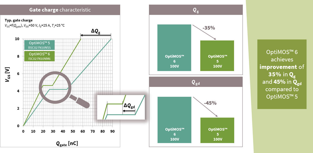
Compared to the well established OptiMOS™ 5 technology, Infineon’s leading thin wafer technology enables significant performance benefits:
- RDS(on) reduced by 18%
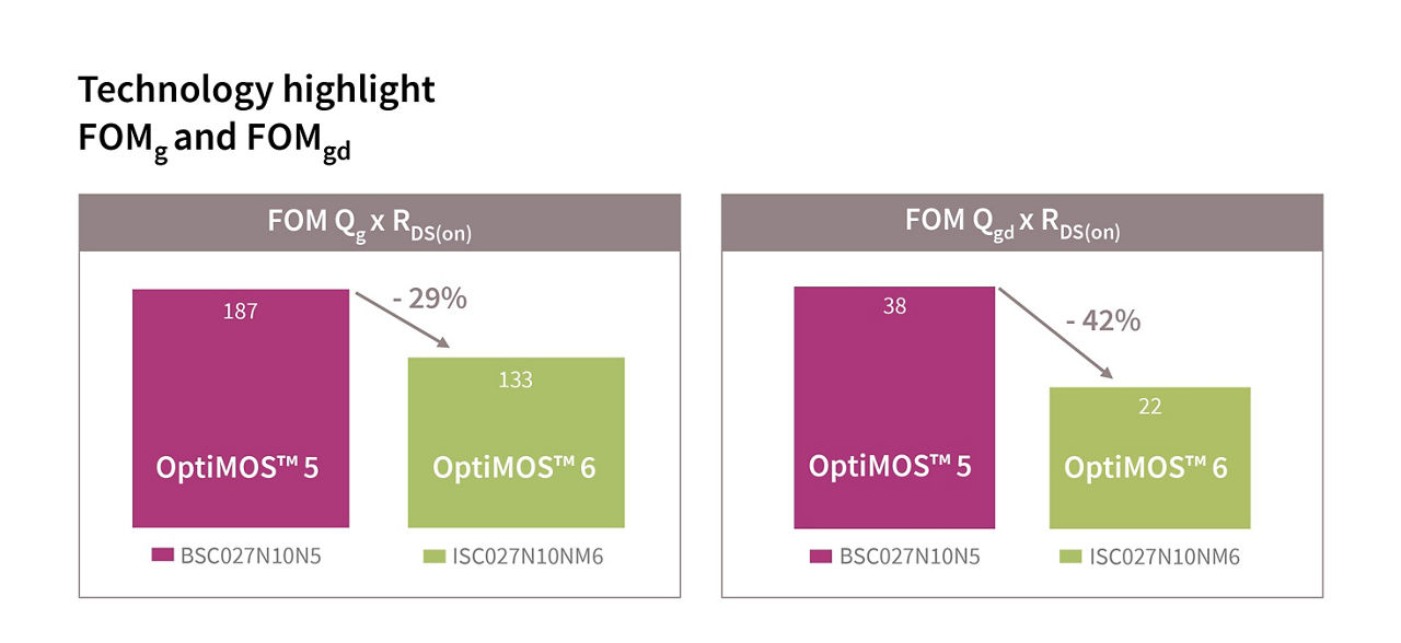
- Improved FOM Qg x RDS(on) by 29% and improved FOM Qgd x RDS(on) by 42%
- Wider Safe Operating Area (SOA)
Infineon’s OptiMOS™ 6 power MOSFET 100 V family is targeting applications such as switch mode power supply (SMPS) as well as solar, power tools, and battery management systems. The enhanced performances yield efficiency improvement, allowing easier thermal design and less paralleling, leading to system cost reduction.
Bring your design to the next level of efficiency
OptiMOS™ 6 100 V is the latest power MOSFET technology completing the Infineon industrial portfolio together with OptiMOS™ 5 and OptiMOS™ 3. These technologies are the perfect fit if you are looking for high performance applications, industry's best figure of merit and high efficiency and power density.
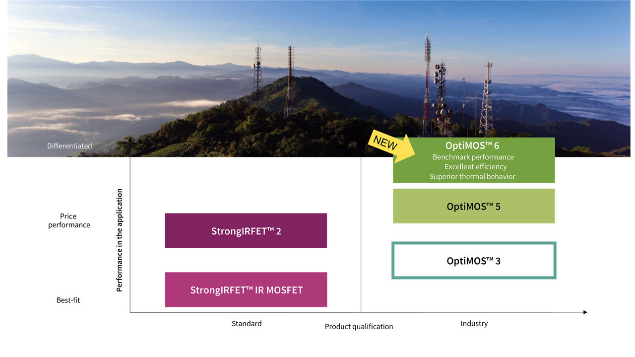
OptiMOS™ 3 is the first generation of 100 V OptiMOS™ MOSFETs. It is recommended for designs allowing large trade-offs between RDS(on) and switching performances.
On the other side OptiMOS™ 5 is considered the price/performance solution and is available in a broad range of packages including very innovative solutions for high power density (Source-Down PQFN 3.3x3.3) or high current capability (TOLx family).
Finally, OptiMOS™ 6 adds to the portfolio a broader choice of RDS(on) ranges with improved figure of merits for lower switching losses and higher power density. The broad portfolio of OptiMOS™ 6 gives the possibility to choose among best-in-class products as well as price/performance solutions.
StrongIRFET™ addresses a wide range of applications. This family is optimized for excellent price/performance, ease of use and broad availability at distribution partners. The main difference between OptiMOS™ and StrongIRFET™ is in the technology performance as well as in the reliability.
StrongIRFET ™ is qualified according to JEDEC for standard application. While the OptiMOS™ family is fully qualified according to JEDEC for industrial application and benefits special customer support such as additional post stress electrical test, extended product change notification window and customer specific requests.
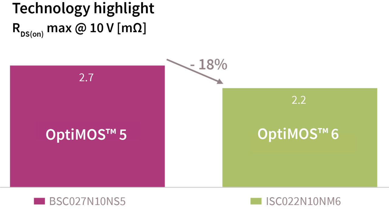
RDS(on) is one of the key parameters of a MOSFET and denotes the on-state resistance measured between drain and source terminals.
A lower RDS(on) value yields:
- Reduction in conduction losses
- Less or avoided paralleling of parts, saving costs and PCB real estate
leading to increased power density!
OptiMOS™ 6 technology in 100 V achieves ~20% lower RDS(on) comparing the best-in-class product ISC022N10NM6 to OptiMOS™ 5 (BSC027N10NS5) in SuperSO8 package.
The improvement in specific on-state resistance brought by OptiMOS™ 6 allows to move to a smaller package (PQFN 3.3x3.3) for the same RDS(on) leading to higher power density.
Total gate charge (Qg) is the amount of charge that needs to be supplied to the gate to turn on (drive) the MOSFET, for some specified conditions. A small value of Qg is highly desirable in high-switching frequency applications, since it directly impacts on the driving losses.
The gate-to-drain charge Qgd represents the part of gate charge associated with the Miller plateau extension, required to complete the drain voltage transition. For the same driving circuit, a lower Qgd means faster voltage transients, hence lower switching losses. This is of utmost importance in high-switching frequency, hard-switched SMPS, where switching losses play a significant role.
Focusing on devices with same RDS(on) of 2.7 mOhm and in SuperSO8 package, the new OptiMOS™ 6 100 V, shows a reduction of 35% in total gate charge compared to OptiMOS™ 5 while at the same time, gate-to-drain charge, is 45% lower, with correspondent benefits in switching losses.
The MOSFET “figure of merit” (FOM) is a performance indicator of a technology which accounts for both conduction and switching losses. FOM is calculated as on-resistance (RDS(on)) times total gate charge (Qg) and is usually expressed in mΩ x nC.
Why is the Figure of Merit an important parameter for technology evaluation?
RDS(on) is a measure of the conduction losses while, on the other hand, total gate charge Qg impacts on both the driving losses and part of switching losses. In order to minimize the total losses, both RDS(on) and Qg need to be minimized.
For every technology, the FOM = RDS(on) x Qg is a given number: it is not possible to improve RDS(on) without impacting the charges, unless FOM is improved as well.
OptiMOS™ 6 100 V shows significant improvement up to 30% in FOM compared to OptiMOS™ 5 100 V. In other words, for the same RDS(on), OptiMOS™ 6 100 V would show 30% lower Qg compared to OptiMOS™ 5 100 V.
Similarly to the FOM, the gate-to-drain charge figure-of-merit FOMgd is a performance indicator of a technology which takes in consideration both conduction and switching losses. FOMgd is calculated as on-resistance (RDS(on)) times gate-to-drain charge (Qgd) and is usually expressed in mΩ x nC.
Why is the FOMgd an important parameter for technology evaluation?
RDS(on) is a measure of the conduction losses while, gate-to-drain charge Qgd impacts on switching losses (especially during turn-off). In order to minimize the total losses, both RDS(on) and Qgd need to be minimized.
OptiMOS™ 6 100 V shows significant improvement up to 42% in FOMgd compared to OptiMOS™ 5 100 V. In other words, for the same RDS(on), OptiMOS™ 6 100 V would show 42% lower Qgd compared to OptiMOS™ 5 100 V.
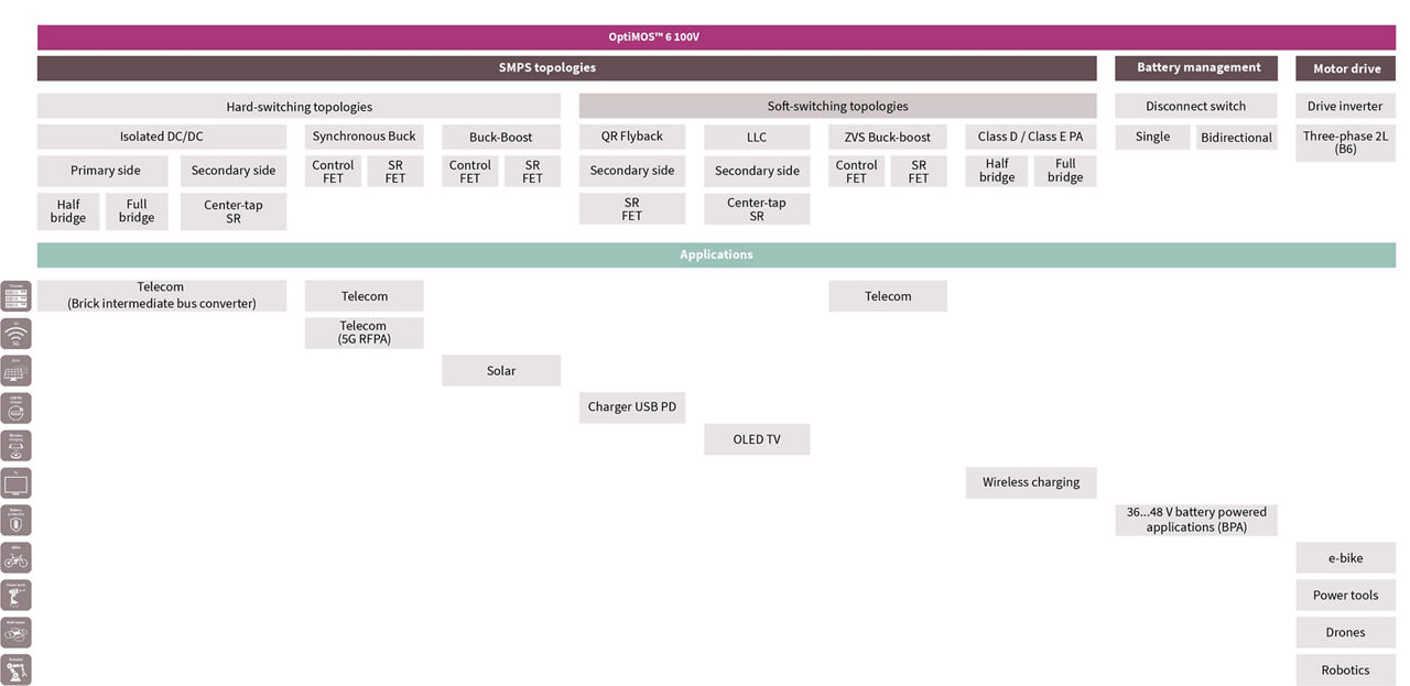
OptiMOS™ 6 100 V has been designed primarily to address high switching frequency applications such as switch mode power supply (e.g. telecom, server, charger, adapter, TV...).
Stay tuned for more information on motor control and solar applications to see all the advantages that this technology can bring!
Soft switching happens when either the voltage or current is zero before the switch is turned on or off. This has benefits, like the reduction of total switching losses. Soft switching is usually a proprieties of resonant converters. In some cases, it would be possible to achieve soft-switching even in hard-switched PWM topologies: one approach is to introduce auxiliary circuits that enable soft switching for the control MOSFET, while recovering the energy otherwise lost and improving the efficiency.
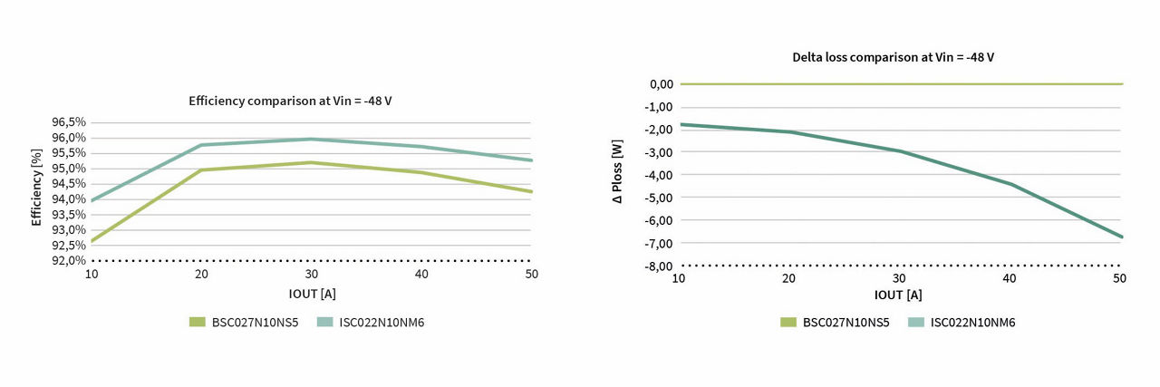
A possible application is a ZVS inverting buck boost -(36...60) V to 12 V DC-DC converter. In this topology, an active clamp circuit recovers, in a lossless way, Qrr from the SR switch towards the output, while achieving ZVS for the control switch.
Best-in-class products in the newly released OptiMOS™ 6 technology (ISC022N10NM6) are compared to OptiMOS™ 5 (BSC027N10NS5) in SuperSO8 (PQFN 5x6) package in this application. The result is stunning: OptiMOS™ 6 in 2.2 mΩ achieves roughly 1% better efficiency across all the line and load conditions, compared to the 2.7 mΩ product in OptiMOS™ 5.
The improvement in efficiency is explainable as the joint contribution of:
- The lower driving losses, thanks to approximatively 20% lower (typ) Qg
- Lower turn-off losses due the lower Qgd – an improvement just shy of 40%
- Lower conduction losses with a 18% lower RDS(on)
The improvement in efficiency lowers the total losses by 7 W, a very remarkable improvement allowing easier thermal management and increased power density. ISC022N10NM6 represents the lowest RDS(on) available in the market for SuperSO8 (PQFN 5x6) package in 100 V.
Hard switching occurs when there is an overlap between voltage and current when switching the transistor on and off.
V x I crossover losses are the main source of losses during turn-off, while Qoss associated losses (due to the charge stored in the output capacitance) dominates the turn-on transient.
In high switching frequency SMPS, switching losses represent a substantial share of the total losses. Turn-off losses are reduced by lowering the gate-to-drain charge Qgd, that would result in a faster voltage transition. Turn-on losses are minimized by a low value for the output charge Qoss.
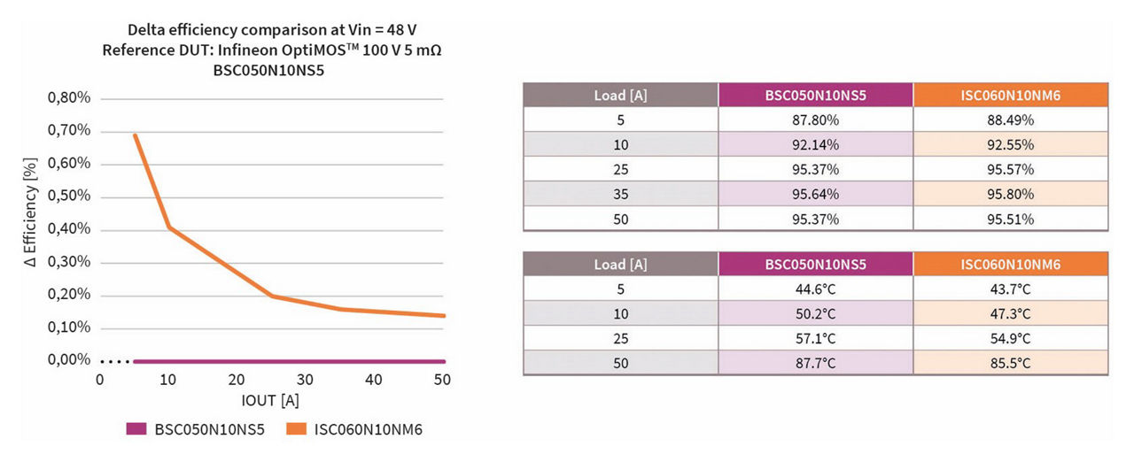
OptiMOS™ 6 100 V, showing leading FOMgd and FOMoss figure of merits, enables remarkable efficiency improvement when compared to the previous available technology. In a telecom quarter brick 250 kHz, 600 W 48 Vin/12 Vout full bridge/full bridge, ISC060N10NM6 (6 mΩ) achieves up to +0.4% better efficiency and lower temperature compared to BSC050N10NS5 (5 mΩ). This benefits in higher system reliability as lower system cost.
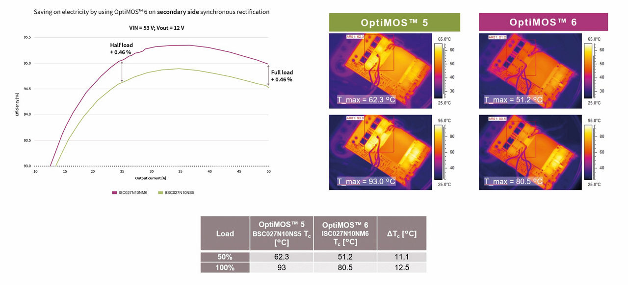
A 250 kHz, 600 W telecom quarter brick 48 Vin/12 Vout full bridge featuring center-tap rectifier was used to compare 2.7 mΩ 100 V SuperSO8 MOSFETs on the secondary side.
ISC027N10NM6 achieved 0.46% better efficiency compared to BSC027N10NS5 which results in about 3 W lower losses.
This directly translates in a dramatic temperature improvement with ~12°C difference at full load, which enables easier thermal designs and improved lifetime up to 75%*
* Estimated value. Reliability model considers GOX breakdown and HTGS drifts
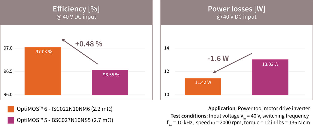
Switching losses in a hard switching converter represent a large share of the total losses in BLDC Motor inverters. For this reason, a good trade-off between RDS(on) and charges Qg and Qgd is needed.
An efficiency comparison between OptiMOS™ 5 (BSC027N10NS5, RDS(on) = 2.7 mΩ) and OptiMOS™ 6 (ISC022N10NM6, RDS(on) = 2.2 mΩ) demonstrated that in this application where conduction losses play a significant role, OptiMOS™ 6 (ISC022N10NM6) was able to achieve better efficiency than OptiMOS™ 5 (BSC027N10NS5) due to lower switching losses and RDS(on). Furthermore, due to the lower turn-off switching losses, the new product produces 10°C lower case temperature at full load compared to the OptiMOS™ 5 version.
These OptiMOS™ 6 power MOSFETs in SuperSO8 package are suitable for battery operated applications requiring efficiency optimization such as power tools, gardening tools, robots and drones.
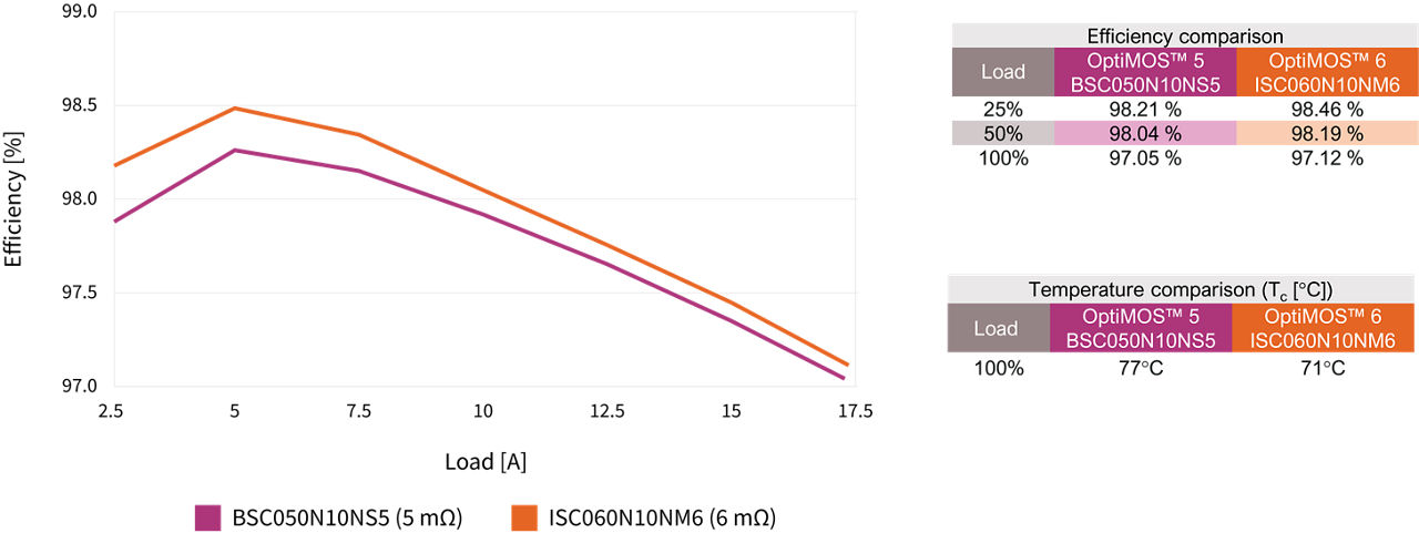
Switching losses in a hard switching converter represent a large share of the total losses in solar power optimizers. For this reason, a good balance between RDS(on) and charges is needed. Recommended products for a power optimizer (synchronous buck stage) are 100 V power MOSFETs in SuperSO8 package, with RDS(on) in the range of 5-6 mΩ.
A efficiency comparison between OptiMOS™ 5 (BSC050N10NS5, RDS(on) = 5 mΩ) and OptiMOS™ 6 (ISC060N10NM6, RDS(on) = 6 mΩ) demonstrated that even with 18 percent higher RDS(on), OptiMOS™ 6 (ISC060N10NM6) achieved better efficiency than OptiMOS™ 5, due to lower switching losses. Furthermore, due to the lower turn-off switching losses, the new product produces 6°C lower case temperature at full load compared to the OptiMOS™ 5 version.
OptiMOS™ 6 100 V is currently available in SuperSO8 and PQFN 3.3x3.3 packages:
Documents
Documents
Get an introduction on the OptiMOS™ 6 – 100 V improvements in key performance parameters such as RDS(on), Qg, Qgd and Safe Operating Area (SOA) compared to the state of the art OptiMOS™ 5 technology.
This video will show the efficiency and thermal comparison of OptiMOS™ 6 vs. OptiMOS™ 5 in a ZVS inverting buck boost DC/DC converter.
This video will provide an overview of the efficiency and thermal behavior of OptiMOS™ 6 vs. OptiMOS™ 5 in a telecom quarter brick intermediate bus converter.
Infineon introduces OptiMOS™ 6 100 V, the new performance MOSFET that enables lower conduction losses and increased power density for the highest performance in the application, meeting contemporary application requirements.
This OptiMOS™ 6 100 V power MOSFET webinar provides an overview of the improved performances and the use case applications that can benefit from this technology such as telecom, solar, and battery powered applications.
Watch now and learn how your applications can benefit from this technology.
Key takeaways:
- Discover the performance of OptiMOS™ 6 100 V MOSFET technology
- Get to know target applications and use case examples in telecom, solar and battery powered applications
- Gain a product portfolio overview
- Learn about key product features and benefits
OptiMOS™ or StrongIRFET™? This is the dilemma!
In most cases we are asking ourselves which one is the best fitting technology for our design.
But how can we make this choice?
Key takeaway:
- Get to know the power discretes portfolio and understand which technology is the best fit for the design
In this video, we will cover the OptiMOS™ 6 100 V through the lens of the telecom/SMPS application.
Key takeaway:
- Understand how OptiMOS™ 6 100 V can bring your SMPS design to next level
OptiMOS™ 6 100 V is the latest power MOSFET technology completing the Infineon industrial portfolio together with OptiMOS™ 5 and OptiMOS™ 3. These technologies are the perfect fit if you are looking for high performance applications, industry's best figure of merit and high efficiency and power density.
OptiMOS™ 3 is the first generation of 100 V OptiMOS™ MOSFETs. It is recommended for designs allowing large trade-offs between RDS(on) and switching performances.
On the other side OptiMOS™ 5 is considered the price/performance solution and is available in a broad range of packages including very innovative solutions for high power density (Source-Down PQFN 3.3x3.3) or high current capability (TOLx family).
Finally, OptiMOS™ 6 adds to the portfolio a broader choice of RDS(on) ranges with improved figure of merits for lower switching losses and higher power density. The broad portfolio of OptiMOS™ 6 gives the possibility to choose among best-in-class products as well as price/performance solutions.
StrongIRFET™ addresses a wide range of applications. This family is optimized for excellent price/performance, ease of use and broad availability at distribution partners. The main difference between OptiMOS™ and StrongIRFET™ is in the technology performance as well as in the reliability.
StrongIRFET ™ is qualified according to JEDEC for standard application. While the OptiMOS™ family is fully qualified according to JEDEC for industrial application and benefits special customer support such as additional post stress electrical test, extended product change notification window and customer specific requests.
RDS(on) is one of the key parameters of a MOSFET and denotes the on-state resistance measured between drain and source terminals.
A lower RDS(on) value yields:
- Reduction in conduction losses
- Less or avoided paralleling of parts, saving costs and PCB real estate
leading to increased power density!
OptiMOS™ 6 technology in 100 V achieves ~20% lower RDS(on) comparing the best-in-class product ISC022N10NM6 to OptiMOS™ 5 (BSC027N10NS5) in SuperSO8 package.
The improvement in specific on-state resistance brought by OptiMOS™ 6 allows to move to a smaller package (PQFN 3.3x3.3) for the same RDS(on) leading to higher power density.
Total gate charge (Qg) is the amount of charge that needs to be supplied to the gate to turn on (drive) the MOSFET, for some specified conditions. A small value of Qg is highly desirable in high-switching frequency applications, since it directly impacts on the driving losses.
The gate-to-drain charge Qgd represents the part of gate charge associated with the Miller plateau extension, required to complete the drain voltage transition. For the same driving circuit, a lower Qgd means faster voltage transients, hence lower switching losses. This is of utmost importance in high-switching frequency, hard-switched SMPS, where switching losses play a significant role.
Focusing on devices with same RDS(on) of 2.7 mOhm and in SuperSO8 package, the new OptiMOS™ 6 100 V, shows a reduction of 35% in total gate charge compared to OptiMOS™ 5 while at the same time, gate-to-drain charge, is 45% lower, with correspondent benefits in switching losses.
The MOSFET “figure of merit” (FOM) is a performance indicator of a technology which accounts for both conduction and switching losses. FOM is calculated as on-resistance (RDS(on)) times total gate charge (Qg) and is usually expressed in mΩ x nC.
Why is the Figure of Merit an important parameter for technology evaluation?
RDS(on) is a measure of the conduction losses while, on the other hand, total gate charge Qg impacts on both the driving losses and part of switching losses. In order to minimize the total losses, both RDS(on) and Qg need to be minimized.
For every technology, the FOM = RDS(on) x Qg is a given number: it is not possible to improve RDS(on) without impacting the charges, unless FOM is improved as well.
OptiMOS™ 6 100 V shows significant improvement up to 30% in FOM compared to OptiMOS™ 5 100 V. In other words, for the same RDS(on), OptiMOS™ 6 100 V would show 30% lower Qg compared to OptiMOS™ 5 100 V.
Similarly to the FOM, the gate-to-drain charge figure-of-merit FOMgd is a performance indicator of a technology which takes in consideration both conduction and switching losses. FOMgd is calculated as on-resistance (RDS(on)) times gate-to-drain charge (Qgd) and is usually expressed in mΩ x nC.
Why is the FOMgd an important parameter for technology evaluation?
RDS(on) is a measure of the conduction losses while, gate-to-drain charge Qgd impacts on switching losses (especially during turn-off). In order to minimize the total losses, both RDS(on) and Qgd need to be minimized.
OptiMOS™ 6 100 V shows significant improvement up to 42% in FOMgd compared to OptiMOS™ 5 100 V. In other words, for the same RDS(on), OptiMOS™ 6 100 V would show 42% lower Qgd compared to OptiMOS™ 5 100 V.
OptiMOS™ 6 100 V has been designed primarily to address high switching frequency applications such as switch mode power supply (e.g. telecom, server, charger, adapter, TV...).
Stay tuned for more information on motor control and solar applications to see all the advantages that this technology can bring!
Soft switching happens when either the voltage or current is zero before the switch is turned on or off. This has benefits, like the reduction of total switching losses. Soft switching is usually a proprieties of resonant converters. In some cases, it would be possible to achieve soft-switching even in hard-switched PWM topologies: one approach is to introduce auxiliary circuits that enable soft switching for the control MOSFET, while recovering the energy otherwise lost and improving the efficiency.
A possible application is a ZVS inverting buck boost -(36...60) V to 12 V DC-DC converter. In this topology, an active clamp circuit recovers, in a lossless way, Qrr from the SR switch towards the output, while achieving ZVS for the control switch.
Best-in-class products in the newly released OptiMOS™ 6 technology (ISC022N10NM6) are compared to OptiMOS™ 5 (BSC027N10NS5) in SuperSO8 (PQFN 5x6) package in this application. The result is stunning: OptiMOS™ 6 in 2.2 mΩ achieves roughly 1% better efficiency across all the line and load conditions, compared to the 2.7 mΩ product in OptiMOS™ 5.
The improvement in efficiency is explainable as the joint contribution of:
- The lower driving losses, thanks to approximatively 20% lower (typ) Qg
- Lower turn-off losses due the lower Qgd – an improvement just shy of 40%
- Lower conduction losses with a 18% lower RDS(on)
The improvement in efficiency lowers the total losses by 7 W, a very remarkable improvement allowing easier thermal management and increased power density. ISC022N10NM6 represents the lowest RDS(on) available in the market for SuperSO8 (PQFN 5x6) package in 100 V.
Hard switching occurs when there is an overlap between voltage and current when switching the transistor on and off.
V x I crossover losses are the main source of losses during turn-off, while Qoss associated losses (due to the charge stored in the output capacitance) dominates the turn-on transient.
In high switching frequency SMPS, switching losses represent a substantial share of the total losses. Turn-off losses are reduced by lowering the gate-to-drain charge Qgd, that would result in a faster voltage transition. Turn-on losses are minimized by a low value for the output charge Qoss.
OptiMOS™ 6 100 V, showing leading FOMgd and FOMoss figure of merits, enables remarkable efficiency improvement when compared to the previous available technology. In a telecom quarter brick 250 kHz, 600 W 48 Vin/12 Vout full bridge/full bridge, ISC060N10NM6 (6 mΩ) achieves up to +0.4% better efficiency and lower temperature compared to BSC050N10NS5 (5 mΩ). This benefits in higher system reliability as lower system cost.
A 250 kHz, 600 W telecom quarter brick 48 Vin/12 Vout full bridge featuring center-tap rectifier was used to compare 2.7 mΩ 100 V SuperSO8 MOSFETs on the secondary side.
ISC027N10NM6 achieved 0.46% better efficiency compared to BSC027N10NS5 which results in about 3 W lower losses.
This directly translates in a dramatic temperature improvement with ~12°C difference at full load, which enables easier thermal designs and improved lifetime up to 75%*
* Estimated value. Reliability model considers GOX breakdown and HTGS drifts
Switching losses in a hard switching converter represent a large share of the total losses in BLDC Motor inverters. For this reason, a good trade-off between RDS(on) and charges Qg and Qgd is needed.
An efficiency comparison between OptiMOS™ 5 (BSC027N10NS5, RDS(on) = 2.7 mΩ) and OptiMOS™ 6 (ISC022N10NM6, RDS(on) = 2.2 mΩ) demonstrated that in this application where conduction losses play a significant role, OptiMOS™ 6 (ISC022N10NM6) was able to achieve better efficiency than OptiMOS™ 5 (BSC027N10NS5) due to lower switching losses and RDS(on). Furthermore, due to the lower turn-off switching losses, the new product produces 10°C lower case temperature at full load compared to the OptiMOS™ 5 version.
These OptiMOS™ 6 power MOSFETs in SuperSO8 package are suitable for battery operated applications requiring efficiency optimization such as power tools, gardening tools, robots and drones.
Switching losses in a hard switching converter represent a large share of the total losses in solar power optimizers. For this reason, a good balance between RDS(on) and charges is needed. Recommended products for a power optimizer (synchronous buck stage) are 100 V power MOSFETs in SuperSO8 package, with RDS(on) in the range of 5-6 mΩ.
A efficiency comparison between OptiMOS™ 5 (BSC050N10NS5, RDS(on) = 5 mΩ) and OptiMOS™ 6 (ISC060N10NM6, RDS(on) = 6 mΩ) demonstrated that even with 18 percent higher RDS(on), OptiMOS™ 6 (ISC060N10NM6) achieved better efficiency than OptiMOS™ 5, due to lower switching losses. Furthermore, due to the lower turn-off switching losses, the new product produces 6°C lower case temperature at full load compared to the OptiMOS™ 5 version.
OptiMOS™ 6 100 V is currently available in SuperSO8 and PQFN 3.3x3.3 packages:
Documents
Documents
Get an introduction on the OptiMOS™ 6 – 100 V improvements in key performance parameters such as RDS(on), Qg, Qgd and Safe Operating Area (SOA) compared to the state of the art OptiMOS™ 5 technology.
This video will show the efficiency and thermal comparison of OptiMOS™ 6 vs. OptiMOS™ 5 in a ZVS inverting buck boost DC/DC converter.
This video will provide an overview of the efficiency and thermal behavior of OptiMOS™ 6 vs. OptiMOS™ 5 in a telecom quarter brick intermediate bus converter.
Infineon introduces OptiMOS™ 6 100 V, the new performance MOSFET that enables lower conduction losses and increased power density for the highest performance in the application, meeting contemporary application requirements.
This OptiMOS™ 6 100 V power MOSFET webinar provides an overview of the improved performances and the use case applications that can benefit from this technology such as telecom, solar, and battery powered applications.
Watch now and learn how your applications can benefit from this technology.
Key takeaways:
- Discover the performance of OptiMOS™ 6 100 V MOSFET technology
- Get to know target applications and use case examples in telecom, solar and battery powered applications
- Gain a product portfolio overview
- Learn about key product features and benefits
OptiMOS™ or StrongIRFET™? This is the dilemma!
In most cases we are asking ourselves which one is the best fitting technology for our design.
But how can we make this choice?
Key takeaway:
- Get to know the power discretes portfolio and understand which technology is the best fit for the design
In this video, we will cover the OptiMOS™ 6 100 V through the lens of the telecom/SMPS application.
Key takeaway:
- Understand how OptiMOS™ 6 100 V can bring your SMPS design to next level