SiC MOSFETディスクリート
650 Vから2000 VまでのCoolSiC™ MOSFETディスクリートは、ハードスイッチングおよび共振スイッチングトポロジーに最適です
インフィニオンのCoolSiC™ SiC MOSFETは、最先端トレンチ半導体プロセスに基づいて構築されており、アプリケーションにおける低損失、ならびに高い動作信頼性を実現するよう最適化されています。ディスクリートCoolSiC™ MOSFET製品は、650 V、1200 V、1700 Vおよび2000 Vの電圧クラスまで、7mΩ~1000mΩのオン抵抗でラインナップをご提供しています。 CoolSiC™トレンチ技術は、柔軟なパラメータ設定が可能で、各製品ラインアップにおけるアプリケーション固有の機能(例えば、ゲートソース電圧、アバランシェ耐量、短絡耐量、ハードコミュテーション用の定格を備えた内蔵ボディダイオード)の実装に使用されます。
インフィニオンの650 V CoolSiC™ MOSFETポートフォリオは、高電流および低容量に最適化されたスイッチング動作を提供し、サーバー、テレコム、モータードライブなど、さまざまな産業用アプリケーション向けに設計されています。1200 V MOSFETシリーズは、オンボードチャージャー/PFC、補助インバータ、無停電電源装置 (UPS) など、産業用および車載用の認定アプリケーションに利用できます。最後に、1700 V CoolSiC™ MOSFETのラインアップは、エネルギー貯蔵システム、高速EV充電、電源管理 (SMPS)、太陽エネルギーシステムのソリューションで使用できるフライバック型で提供されます。2000 V CoolSiC™ MOSFETでは電力密度や過電圧マージンを向上しており、高速EV充電や太陽光発電ソリューションなどの高電圧アプリケーションに最適です。
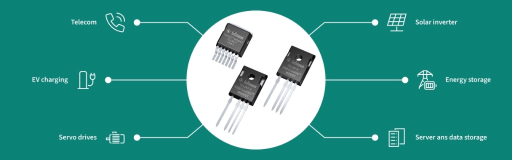
ディスクリートパッケージのCoolSiC™ MOSFETは、力率改善(PFC)回路、双方向トポロジ、DC/DCコンバータ、DC/ACインバータなど、ハードウェアトポロジおよび共振スイッチングトポロジの両方に最適です。不要な寄生ターンオン効果に対する優れた耐性により、ブリッジトポロジのターンオフ電圧が0Vであっても、低ダイナミック損失のベンチマークを実現します。インフィニオンのTOパッケージおよびSMDパッケージ製品には、スイッチング性能最適化用のケルビンソースピンも追加できます。
インフィニオンは、超高速SiC MOSFETスイッチング機能の要求を満たす、厳選されたドライバIC製品を取り揃え、SiCディスクリート製品を完成させています。CoolSiC™ MOSFETとEiceDRIVER™ゲートドライバICは、高効率、小型化、軽量化、部品点数の削減、高いシステム信頼性といったSiC技術の利点を活かしています。
ディスクリートハウジングのCoolSiC™ MOSFETは還流ダイオードを内蔵しているため、追加のダイオードチップを要することなくハードスイッチングが可能です。MOSFETはユニーポーラ特性を持つことから、特に部分負荷状態ではスイッチング損失は温度に依存することなくきわめて低く、導通損失も低いという特徴があります。
インフィニオン独自のSiC (炭化ケイ素)テクノロジーであるCoolSiC™ MOSFETのディスクリート製品は、LLCやZVSのようなハードスイッチングや共振スイッチングのトポロジーに最適で、ゲートドライバーでIGBTやCoolMOS™(Si MOSFET)のように駆動することができます。これらの堅牢なデバイスは、最先端のトレンチ設計により実現される卓越したゲート酸化膜信頼性、クラス最小レベルのスイッチング損失と導通損失、最高の相互コンダクタンスレベル(利得)、しきい値電圧Vth=4V、短絡耐量を提供します。


SiC MOSFET 1200VゲートドライバIC
CoolSiC™ MOSFETのような超高速スイッチングのパワートランジスタは、絶縁ゲート出力部を使うと取り扱いが容易です。その最適解としてインフィニオンのコアレストランス技術に基づくガルバニック絶縁EiceDRIVER™ ICを勧めします。
Key takeaways
- Be familiar with the target applications for CoolSiC™ MOSFET 750 V
- Know the key features and recognize the benefits
- Understand its positioning compared to other technologies
- Know where to find support material and more information
This video highlights the benefits of CoolSiC™, as seen through the eyes of our customers. Featuring testimonials from alpitronic, Tritium, Lite-On, Siemens Mobility, and Fronius, we see how SiC is driving innovation in energy generation, storage, and consumption.
We are introducing the CoolSiC™ MOSFET with .XT interconnection technology in a 1200 V optimized D2PAK-7 SMD package. SiC MOSFET ohmic conduction losses and fully controllable switching transients are a perfect match with the load profile of such motors. Since the SMD device enables passive cooling for the inverters, they can now be designed maintenance-free.
The presentation will inform you about the specifics of the device. Additionally, the presenting expert will give insights about how maintenance-free inverters can be build up. He will also touch other applications, which are profiting from the CoolSiC™ SMD MOSFET.
Dr. Steffen Metzger explains the technical details of the CoolSiC™ MOSFET in 650V, and highlights the benefits they bring for specific applications. Additionally, he compares the 650 V CoolSiC™ MOSFET with GoolGaN™ and CoolMOS™ and their respective positioning within the greater realm of power semiconductors.
最新のCoolSiC™ MOSFET 650Vは、アプリケーションにおけるきわめて低い損失、動作におけるきわめて高い信頼性の両方を妥協することなく最適化した最先端のトレンチ半導体プロセスに基づいています。シリコンカーバイドの強い物理特性をさらに強化したことで、デバイスの性能、堅牢性、使い易さを改善する独自の特長を備えています。
その技術的性質により、CoolSiC™はハイパワーアプリケーションに最適です。CoolSiC™は、高い性能、堅牢性、使い易さを兼ね備え、業界標準となっています。特に高温や厳しい環境下で信頼性の向上を可能にします。CoolSiC™がもたらす利点の詳細について、このビデオをご覧ください。
Key takeaways
- Be familiar with the target applications for CoolSiC™ MOSFET 750 V
- Know the key features and recognize the benefits
- Understand its positioning compared to other technologies
- Know where to find support material and more information
Discover the benefits and challenges associated with connecting SiC power MOSFETs in parallel
This training talks about the integration of motors and drives with Infineon’s CoolSiC™ MOSFET and how this can help you overcome the limitations of traditional solutions.
This training provides an overview of the 2000 V discrete CoolSiC™ family and explains why it is a right fit for high-power applications.
The switching performance in particular is influenced by the chip's inherent properties, the device's operating conditions and the external circuitry. Optimizing operating conditions and circuitry can significantly improve the device performance in an application.
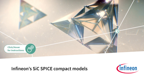
Circuit designers benefit from SPICE compact models that they can use in computer simulation to understand, troubleshoot and optimize the static and dynamic device behavior of applications through virtual prototyping.
This training explains the characteristics and use cases of simulation models offered by Infineon for CoolSiC™ MOSFETs, what to use them for and how to use them effectively.
- The key features and benefits of the 1200 V CoolSiC™ MOSFET in TO247-4 lead package
- How it addresses the market challenges

Did you know statistics show that the rise in population and economy will drive energy demand to increase by 58% by 2040?
Also, the current climate concerns and geopolitical instability make it even more attractive than ever to generate green, sustainable, and efficient energy, right from home!
Photovoltaic technology, for example, provides a new level of energy independence. Like few other energy sources, solar is accessible directly by consumers and communities, allowing them to build small, independent power grids for personal or collective use.
It is here that Infineon can assist our customers by providing the best-in-class solutions for each application!

As mentioned in the first part, beside social and economic reasons, climate concerns and geopolitical instability make the possibility of generating green, sustainable, and efficient energy right from home very attractive and desirable, and photovoltaic technology provides that level of energy independence.
With that in mind, Infineon is ready to assist our customers, by providing the best-in-class solutions for each application!
Stay tuned, to learn more about it!
By taking this course you will learn more about…
- The gate driving limitation in SiC MOSFETs
- The reason for gate driving limitation parameters in datasheets
- The possible solution to overcome those issues and improve the reliability
Understand why to use WBG switches for bi-directional converters, the topologies used and how they function.
If you want to be an expert of CoolSiC™ discretes and the .XT technology, watch this video!
With the growing market of electrical vehicles, the industry has put forward more requirements for the performance of charging piles.
This e-learning will show you that the emergence of CoolSiC™ MOSFETs has improved the charging pile industry to make the EV charger smaller, faster and with higher efficiency.
This training will introduce you to how the CoolSiC™ will help to design the next generation of servo drives.
Driving a CoolSiC™ MOSFET is much easier than you think. This training will show you how it can be driven with a 0 V turn-off gate voltage.
With this training you will learn how to calculate a reference gate resistance value for your Silicon Carbide MOSFET, how to identify suitable gate driving ICs based on peak current and power dissipation requirements and to fine-tune the gate resistance value in laboratory environment based on worst case conditions.
See how to optimize devices’ behavior in their applications with Infineon’s SPICE Compact Models for CoolSiC™ MOSFETs.
In this video, you will focus on the comparison of the power handling capacity of IGBTs and SiC MOSFETs, Go through the different aspects that need to be considered when dimensioning an IGBT or a MOSFET for a certain application.
- Distinguish the features and benefits of Infineon’s CoolSiC™ solutions in target applications and identify Infineon’s fully scalable CoolSiC™ portfolio to meet this automotive market transition
- Learn about the reasons for the increasing introduction of silicon carbide technology in the automotive applications
By watching this eLearning you will:
- Understand package inductance
- Know why wide bandgap transistors are more susceptible to package inductance, and
- Identify which Infineon package types have lower inductance
Infineon offers trusted expertise in all 3 main power semiconductor technologies. Check out how to position them in AC-DC applications!
Click here to find out more.
Infineon 650V CoolSiC™ MOSFETs offer a perfect response to the progressing mega trends: more efficiency and power density.
Click here to find out more.
650 V CoolSiC™ technology parameters in a straight comparison with the 600 V CoolMOS™ CFD7.
Click here to find out more.
Get familiar with the main target topologies and the benefits 650 V CoolSiC™ has to offer.
Click here to find out more.
Understand critical design information in order to get the best out of the 650 V CoolSiC™.
Click here to find out more.