- ASIC
- バッテリー マネージメントIC
- クロックとタイミングソリューション
- ESDおよびサージ保護デバイス
- 自動車用イーサネット
- 評価ボード
- 高信頼性(HiRel)
- アイソレーター
- メモリ
- マイクロコントローラー
- パワー
- RF
- セキュリティ ソリューションおよびスマートカードソリューション
- センサー技術
- 小信号トランジスタおよびダイオード
- トランシーバー
- ユニバーサル シリアル バス(USB)
- ワイヤレス接続
- Search Tools
- Technology
- Packages
- Product Information
- ご注文
- 概要
- 組込みフラッシュIPソリューション
- フラッシュプラスRAM MCPソリューション
- F-RAM (強誘電体RAM)
- NORフラッシュ
- nvSRAM (不揮発性 SRAM)
- PSRAM – 擬似スタティックRAM
- 耐放射線・高信頼性メモリ
- SRAM (スタティック RAM)
- ウェーハおよびダイメモリソリューション
- 概要
- 32ビットFM Arm® Cortex® マイクロコントローラー
- 32ビットAURIX™ TriCore™マイクロコントローラー
- 32ビットPSOC™ Arm® Cortex® マイクロコントローラー
- 32ビット TRAVEO™ T2G Arm® Cortex® マイクロコントローラー
- 32ビットXMC™産業用マイクロコントローラー Arm® Cortex®-M
- レガシー マイクロコントローラー
- モーター制御SoC/SiP
- センシングコントローラー
- 概要
- AC-DC電力変換
- 従来型の車載パワートレインIC
- クラスD オーディオアンプIC
- 非接触パワー&センシングIC
- DC/DCコンバーター
- ダイオードとサイリスタ (Si/SiC)
- 窒化ガリウム(GaN)
- ゲートドライバIC
- IGBT – 絶縁ゲート型バイポーラトランジスタ
- インテリジェント パワーモジュール (IPM)
- LEDドライバIC
- モータードライバ
- MOSFET
- パワーモジュール
- 電源IC
- 保護および監視IC
- シリコンカーバイド (SiC)
- スマート パワー スイッチ
- ソリッドステートリレー (SSR)
- ワイヤレス充電IC
- 概要
- アンテナクロススイッチ
- アンテナチューナー
- バイアスと制御
- カプラ
- ドライバアンプ
- 耐放射線マイクロ波とRF
- ローノイズアンプ (LNA)
- 高周波ダイオード
- RFスイッチ
- RFトランジスタ
- ワイヤレス制御向けレシーバー
- 概要
- Calypso®製品
- CIPURSE™ 製品
- 非接触メモリ
- OPTIGA™の組込みセキュリティ ソリューションの詳細
- SECORA™セキュリティソリューション
- セキュリ ティコントローラー
- スマートカードモジュール
- 政府ID向けスマートソリューション
- 概要
- USB 2.0 ペリフェラル コントローラー
- USB 3.2 ペリフェラル コントローラー
- USB ハブ コントローラー
- USB PD高電圧マイクロコントローラー
- USB-C AC-DC および DC-DC 充電ソリューション
- USB-C充電ポートコントローラー
- USB-Cパワーデリバリー コントローラー
- 概要
- AIROC™ オートモーティブワイヤレス
- AIROC™ Bluetooth®およびマルチプロトコル
- AIROC™ コネクトテッドMCU
- AIROC™ Wi-Fi + Bluetooth®コンボ
- 概要
- FM0+ 32ビット Arm® Cortex®-M0+ マイクロコントローラー (MCU)
-
FM3 32ビットArm® Cortex-M3®マイクロコントローラー (MCU) ファミリー
- 概要
- FM3 CY9AFx1xKシリーズ Arm® Cortex®-M3マイクロコントローラー (MCU)
- FM3 CY9AFx1xL/M/N シリーズ Arm® Cortex®-M3マイクロコントローラー (MCU)
- FM3 CY9AFx2xK/L シリーズ Arm® Cortex®-M3マイクロコントローラー (MCU)
- FM3 CY9AFx3xK/L シリーズ 超低リーク Arm® Cortex®-M3マイクロコントローラー (MCU)
- FM3 CY9AFx4xL/M/N シリーズ 低消費電力 Arm® Cortex®-M3マイクロコントローラー (MCU)
- FM3 CY9AFx5xM/N/Rシリーズ 低消費電力 Arm® Cortex®-M3マイクロコントローラー (MCU)
- FM3 CY9AFxAxL/M/N シリーズ 超低リーク Arm® Cortex®-M3 マイクロコントローラー (MCU)
- FM3 CY9BFx1xN/R 高性能シリーズ Arm® Cortex®-M3マイクロコントローラー (MCU)
- FM3 CY9BFx1xS/T 高性能シリーズ Arm® Cortex®-M3マイクロコントローラー (MCU)
- FM3 CY9BFx2xJシリーズ Arm® Cortex®-M3マイクロコントローラー (MCU)
- FM3 CY9BFx2xK/L/Mシリーズ Arm® Cortex®-M3マイクロコントローラー (MCU)
- FM3 CY9BFx2xS/Tシリーズ Arm® Cortex®-M3マイクロコントローラー (MCU)
- FM4 32ビットArm® Cortex-M4®マイクロコントローラー (MCU) ファミリー
- 概要
-
32 ビット TriCore™ AURIX™ – TC2x
- 概要
- AURIX™ ファミリー – TC21xL
- AURIX™ファミリー – TC21xSC (ワイヤレス充電)
- AURIX™ ファミリー – TC22xL
- AURIX™ ファミリー – TC23xL
- AURIX™ ファミリー – TC23xLA (ADAS)
- AURIX™ ファミリー – TC23xLX
- AURIX™ ファミリー – TC264DA (ADAS)
- AURIX™ ファミリー – TC26xD
- AURIX™ ファミリー – TC27xT
- AURIX™ ファミリー – TC297TA (ADAS)
- AURIX™ ファミリー – TC29xT
- AURIX™ファミリー – TC29xTT (ADAS)
- AURIX™ ファミリー – TC29xTX
- AURIX™ TC2xx (エミュレーションデバイス)
-
32 ビット TriCore™ AURIX™ – TC3x
- 概要
- AURIX™ ファミリー TC32xLP
- AURIX™ ファミリー – TC33xDA
- AURIX™ ファミリー - TC33xLP
- AURIX™ ファミリー – TC35xTA (ADAS)
- AURIX™ ファミリー – TC36xDP
- AURIX™ ファミリー – TC37xTP
- AURIX™ ファミリー – TC37xTX
- AURIX™ ファミリー – TC38xQP
- AURIX™ ファミリー – TC39xXA (ADAS)
- AURIX™ ファミリー – TC39xXX
- AURIX™ ファミリー – TC3Ex
- AURIX™ TC37xTE (エミュレーションデバイス)
- AURIX™ TC39xXE (エミュレーションデバイス)
- 32 ビット TriCore™ AURIX™ - TC4x
- 概要
- PSOC™ 4 Arm® Cortex® -M0/M0+
- PSOC™ 4 HV Arm® Cortex® -M0+
- PSOC™ 5 LP Arm® Cortex® -M3
- PSOC™ 6 Arm® Cortex®-M4 / M0+
- PSOC™マルチタッチタッチスクリーンコントローラー
- PSOC™ Control C3 Arm® Cortex®-M33
- 自動車用PSOC™ 4 Arm® Cortex®-M0/M0+
- PSOC™ Edge Arm® Cortex® M55/M33
- 概要
- ボディ用32ビットTRAVEO™T2G Arm® Cortex®
- クラスター用の 32 ビット TRAVEO™ T2G Arm® Cortex®
- 概要
- 32ビットXMC1000産業用マイクロコントローラー Arm® Cortex®-M0
- Cortex-M4® Arm® 32ビットXMC4000産業用マイクロコントローラー
- XMC5000産業用マイクロコントローラーArm® Cortex® -M4F
- 32ビットXMC7000産業用マイクロコントローラー Arm® Cortex®-M7®
- 概要
- 整流ブリッジおよびACスイッチ
- CoolSiC™ ショットキーダイオード
- ダイオードベアダイ
- Si ダイオード
- サイリスタ/ダイオード パワーモジュール
- サイリスタソフトスタータモジュール
- サイリスタ / ダイオードディスク
- 概要
- 車載ゲートドライバ IC
- ガルバニック絶縁型ゲートドライバ
- GaN HEMT用ゲートドライバIC
- ハイサイドゲートドライバ
- レベルシフト
- ローサイド ドライバ
- トランスドライバIC
- 概要
- BLDCモータードライバ
- BDCモータードライバ
- ステッピングモーターおよびサーボモーター ドライバ
- MCU搭載モータードライバ
- MOSFETを使用したブリッジドライバ
- ゲートドライバIC
- 概要
- 車載用MOSFET
- デュアルMOSFET
- MOSFET(Si&SiC)モジュール
- NチャネルデプレッションモードMOSFET
- NチャネルMOSFET
- PチャネルMOSFET
- CoolSiC™ MOSFET
- 小信号/小電力MOSFET
- 概要
- 車載用トランシーバー
- OPTIREG™リニア電圧レギュレーター (LDO)
- OPTIREG™ PMIC
- OPTIREG™スイッチャー
- OPTIREG™ システム ベーシス チップ (SBC)
- 概要
- EZ-USB™ CX3 MIPI CSI-2 to USB 5 Gbps カメラ コントローラー
- EZ-USB™ FX10 & FX5N USB 10Gbpsペリフェラルコントローラ
- EZ-USB™ FX20 USB 20 Gbpsペリフェラルコントローラー
- EZ-USB™ FX3 USB 5 Gbps ペリフェラル コントローラー
- EZ-USB™ FX3S USB 5 Gbps ペリフェラル コントローラー (ストレージ インターフェース付き)
- EZ-USB™ FX5 USB 5 Gbpsペリフェラルコントローラー
- EZ-USB™ SD3 USB 5 Gbps ストレージコントローラー
- EZ-USB™ SX3: FIFOインターフェースの USB 5 Gbps ペリフェラル コントローラー
- 概要
- EZ-PD™ CCG3 USB Type-Cポート コントローラーPD
- EZ-PD™ CCG3PA USB-C および PD
- EZ-PD™ CCG3PA-NFET USB-C PD コントローラー
- EZ-PD™ CCG7x シングルポート USB-Cパワーデリバリーおよび DC-DC コントローラー
- EZ-PD™ PAG1: 第 1 世代電源アダプター
- EZ-PD™ PAG2: 第 2 世代電源アダプター
- EZ-PD™ PAG2-PD USB-C PD コントローラー
- 概要
- EZ-PD™ ACG1F 1ポートUSB-Cコントローラー
- EZ-PD™ CCG2 USB Type-Cポート コントローラー
- EZ-PD™ CCG3PA車載用USB-Cおよびパワーデリバリーコントローラー
- EZ-PD™ CCG4 2 ポートUSB-CおよびPD
- EZ-PD™ CCG5デュアルポートおよび CCG5C シングルポート USB-C PDコントローラー
- EZ-PD™ CCG6 1ポート USB-C & PDコントローラー
- EZ-PD™ CCG6_CFP および EZ-PD™ CCG8_CFPデュアルシングルポート USB-C PD
- EZ-PD™ CCG6DFデュアルポートおよびCCG6SFシングルポートUSB-C PDコントローラー
- EZ-PD™ CCG7D車載用デュアルポートUSB-C PD + DC-DCコントローラー
- EZ-PD™ CCG7S車載用シングルポートUSB-C PDソリューション (DC-DCコントローラーおよびFET内蔵)
- EZ-PD™ CCG8デュアル シングル ポートUSB-C PD
- EZ-PD™ CMG1 USB-C EMCAコントローラー
- 拡張パワーレンジ (EPR) 搭載EZ-PD™ CMG2 USB-C EMCA
- 最新情報
- 航空宇宙および防衛
- AIとデータセンター
- 自動車
- 通信
- 民生用電子機器
- ヘルスケアとライフスタイル
- 家電製品
- 産業用アプリケーション
- 再生可能エネルギー
- ロボティックス
- セキュリティソリューション
- スマートホームとスマートビルディング
- ソリューション
- 概要
- 電源アダプターと充電器
- スマートテレビ向けの完全なシステムソリューション
- モバイルデバイスとスマートフォンソリューション
- マルチコプターとドローン
- 電動工具
- ホームエンターテインメント アプリケーション向けの半導体ソリューション
- スマート会議システム
- 概要
- Digital health
- 資産管理の追跡
- バッテリーの形成とテスト
- 電動フォークリフト
- バッテリー蓄電 (BESS)
- EV充電
- 高電圧ソリッドステート配電
- 産業用オートメーション
- 産業用モータードライブおよび制御
- 産業用ロボット
- LED 照明システムの設計
- 小型電気自動車ソリューション
- 電動工具
- 送配電
- トラクション
- 無停電電源装置 (UPS)
- Digital health
- 概要
- バッテリーの形成とテスト
- EV充電
- 水素
- 太陽光発電
- 風力
- ソリッドステート サーキット ブレーカー (SSCB)
- バッテリー蓄電 (BESS)
- 概要
- デバイス認証とブランド保護
- モノのインターネット (IoT) 向けの組み込みセキュリティ
- eSIM アプリケーション
- 公的身分証明書
- モバイルセキュリティ
- 決済ソリューション
- アクセス管理および発券ソリューション
- 概要
- 家庭用ロボット
- 空調システム (HVAC)
- ホームオートメーションとビルオートメーション
- PCアクセサリ
- ホームエンターテインメント アプリケーション向けの半導体ソリューション
- 概要
- 車載用補助システム
- 車載ゲートウェイ
- 車載用パワー分配システム
- ボディコントロールモジュール(BCM)
- コンフォート&コンビニエンス エレクトロニクス
- ゾーンDC-DCコンバーター 48 V~12 V
- ゾーンコントロールユニット
- 概要
- アクティブサスペンションコントロール
- 車載用ブレーキング ソリューション
- 車載用ステアリング ソリューション
- シャーシ ドメイン制御
- 最新情報
- デジタル ドキュメンテーション
- 評価ボード
- ファインダー & セレクション ツール
- プラットフォーム
- サービス
- インフィニオン オンライン パワー シミュレーション プラットフォーム
- ソフトウェア
- ツール
- パートナー
- インフィニオン フォー メーカーズ
- ユニバーシティ アライアンス プログラム
- 概要
- AIROC™ ソフトウェアとツール
- AURIX™のツールとソフトウェア
- 自動車ソフトウェア開発用のDRIVECORE
- iMOTION™ ツールとソフトウェア
- インフィニオンのスマートパワースイッチおよびゲートドライバ ツールスイート
- MOTIX™ ソフトウェア&ツール
- OPTIGA™ ツールとソフトウェア
- PSOC™ ソフトウェアとツール
- TRAVEO™ ソフトウェアとツール
- XENSIV™ツールおよびソフトウェア
- XMC™ ツールとソフトウェア
- 概要
- IPOSIM オンライン パワー シミュレーション プラットフォーム
- CoolGaN™シミュレーションツール(PLECS)
- HiRel フィット レート ツール
- IPOSIM オンライン パワー シミュレーション プラットフォーム
- インフィニオン デザイナー
- インタラクティブな製品シート
- IPOSIM オンライン パワー シミュレーション プラットフォーム
- InfineonSpiceオフラインシミュレーションツール
- OPTIREG™ 車載電源IC シミュレーションツール (PLECS)
- パワーMOSFETシミュレーション モデル
- PowerEsimスイッチモード電源設計ツール
- ソリューションファインダー
- XENSIV™磁気センサー シミュレーション ツール
- 概要
- AURIX™認証
- AURIX™開発ツール
- AURIX™組込みソフトウェア
- AURIX™マイクロコントローラーキット
- 概要
- CAPSENSE™コントローラー コンフィギュレーション ツール EZ-Click
- DC-DC統合POL電圧レギュレーター設定ツール – PowIRCenter
- EZ-USB™ SX3コンフィギュレーション ユーティリティ
- FM+ コンフィギュレーション ツール
- FMx設定ツール
- トランシーバーICコンフィギュレーション ツール
- USB EZ-PD™コンフィギュレーション ユーティリティ
- USB EZ-PD™コンフィギュレーション ユーティリティ
- USB EZ-USB™ HX3C Blaster Plusコンフィギュレーション ユーティリティ
- USB UARTコンフィギュレーション ユーティリティ
- XENSIV™タイヤ空気圧センサーのプログラミング
- 概要
- EZ-PD™ CCGx Dock ソフトウェア開発キット
- FMx Softune IDE
- ModusToolbox™ ソフトウェア
- PSOC™ ソフトウェア
- レーダー開発キット
- 錆
- USBコントローラーSDK
- ワイヤレス接続 Bluetooth メッシュヘルパー アプリケーション
- XMC™ DAVE™ソフトウェア
- 概要
- AIROC™ Bluetooth® Connect Appアーカイブ
- Cypress™ Programmerのアーカイブ
- EZ-PD™ CCGx 電力ソフトウェア開発キットのアーカイブ
- ModusToolbox™ ソフトウェアのアーカイブ
- PSOC™ Creatorのアーカイブ
- PSOC™ Designerのアーカイブ
- PSOC™ Programmerのアーカイブ
- USB EZ-PD™コンフィギュレーション ユーティリティ アーカイブ
- USB EZ-PD™ホストSDKのアーカイブ
- USB EZ-USB™ FX3のアーカイブ
- EZ-USB™ HX3PD コンフィギュレーション ユーティリティ
- WICED™ Smart SDKのアーカイブ
- WICED™ Studioのアーカイブ
- 最新情報
- サポート
- トレーニング
- 開発者コミュニティ
- News
ビジネス&財務プレス
2026/04/07
ビジネス&財務プレス
2026/03/30
ビジネス&財務プレス
2026/03/10
ビジネス&財務プレス
2026/03/09
- 会社概要
- 私たちのストーリー
- イベント
- プレス
- 投資家向け情報
- 採用情報
- 品質
- 最新ニュース
ビジネス&財務プレス
2026/04/07
ビジネス&財務プレス
2026/03/30
ビジネス&財務プレス
2026/03/10
ビジネス&財務プレス
2026/03/09
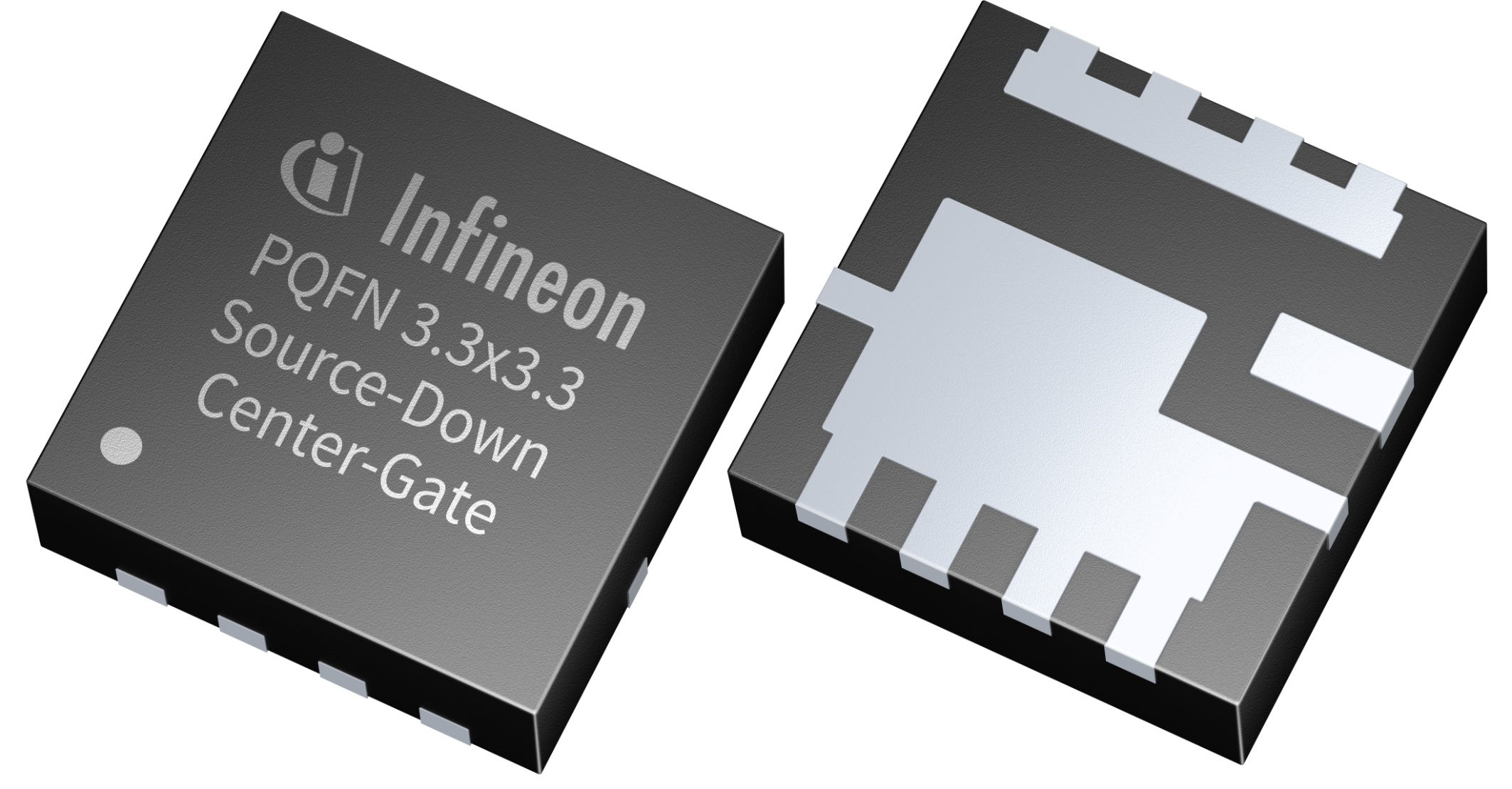
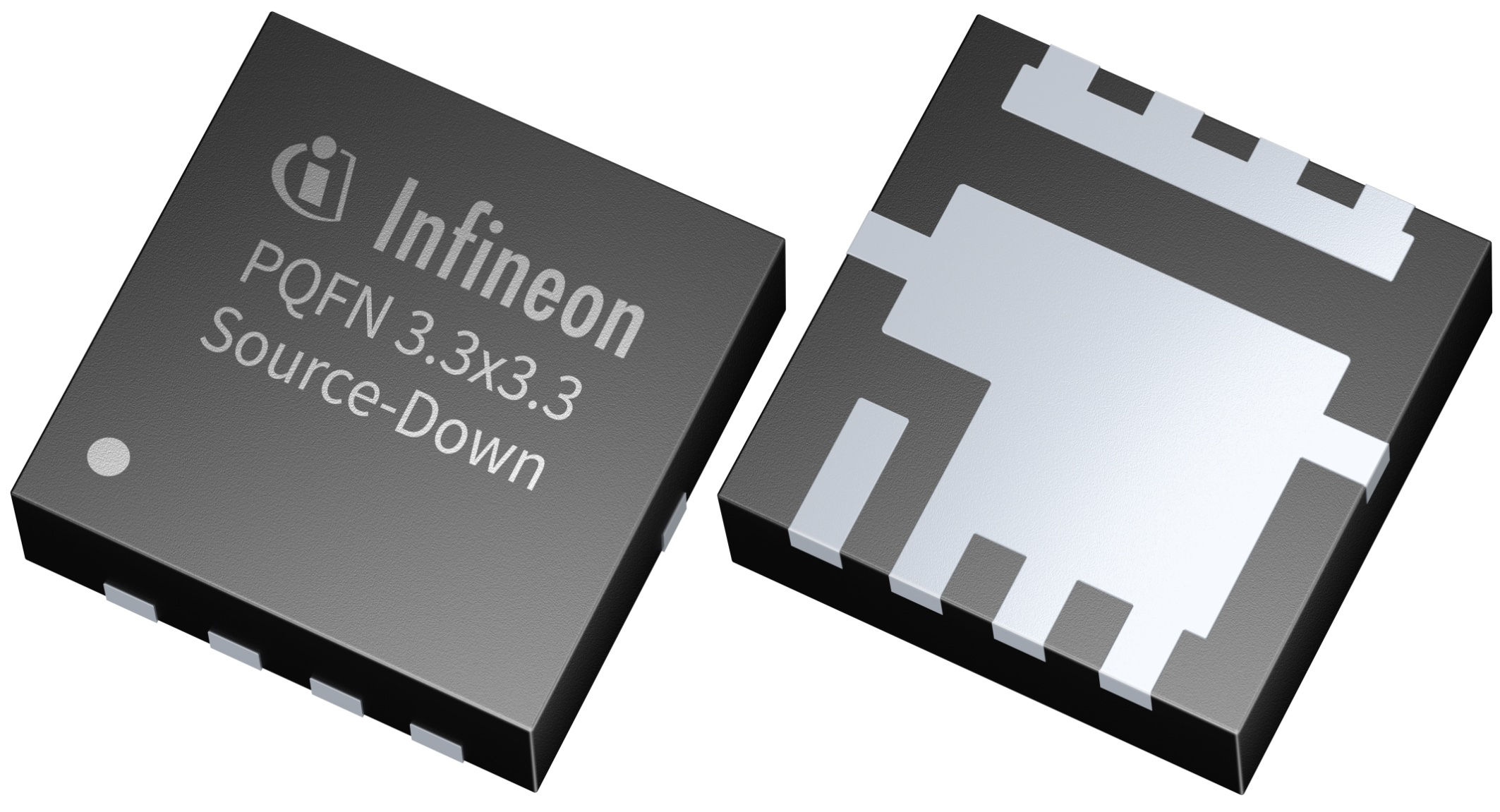
インフィニオン、3.3 x 3.3 mm 2 のPQFN の新しいOptiMOS™ パワーMOSFET パッケージにより、25 V から100 V のバリエーションで革新的なソースダウンテクノロジーを実現
マーケットニュース
2022 年1 月7 日、ミュンヘン(ドイツ)
高電力密度、最適化された性能、そして使い易さは、最新の電力システムを設計する際に重要な要件となります。エンドアプリケーションにおける設計上の課題に対する実用的なソリューションを提供するため、インフィニオン テクノロジーズ AG (FSE: IFX / OTCQX: IFNNY) は、25~100 V の幅広い電圧に対応した、PQFN 3.3 x 3.3 mm 2 パッケージのOptiMOS™ソースダウン (SD) パワーMOSFET を発表しました。このパッケージは、高効率、高電力密度、優れた熱管理、低BOM を実現し、パワーMOSFET の性能における新たな標準を設定します。PQFNは、 モータードライブ、 サーバや テレコム用の SMPS、ORリング、 バッテリーマネジメントシステムなどのアプリケーションに対応しています。
標準的なドレインダウンのコンセプトと比較して、最新のソースダウンパッケージ技術は、同じパッケージ外形で、より大きなシリコンダイの搭載を可能にします。さらに、デバイスの全体的な性能を制限しているパッケージによる損失も削減することができます。これにより、従来のドレインダウンパッケージと比較して、
R DS (on) を最大30%削減することができます。システムレベルでは、SuperSO8 5 x 6 mm 2 のフットプリントからPQFN 3.3 x 3.3 mm 2 パッケージに移行し、約65%のスペース削減が可能で、フォームファクターの縮小がメリットとして挙げられます。これにより、利用可能なスペースをより有効に活用することができ、エンドシステムにおける電力密度やシステム効率を向上させることができます。
さらに、ソースダウンコンセプトでは、熱をボンドワイヤーや銅クリップ経由ではなく、サーマルパッドを通して直接プリント基板に放熱します。熱抵抗 R thJC が1.8K/W から1.4K/W へと20%以上改善され、熱管理の簡素化が可能になります。インフィニオンは、SD 標準ゲートとSD センターゲートの2 種類のフットプリントとレイアウトオプションを提供しています。標準ゲートレイアウトは、ドレインダウンパッケージのドロップイン置換を簡素化し、センターゲートレイアウトは最適かつ容易な並列化を可能にします。これらの2 つのオプションは、PCB における最適なデバイス配置、PCB 寄生要素の最適化、および使い易さをもたらすことができます。
供給について
25~100 V の幅広い電圧に対応した、PQFN 3.3 x 3.3 mm 2 パッケージのOptiMOS™ソースダウン型パワーMOSFET は、2 種類のフットプリントバージョンで提供を開始いたしました。
製品の詳細については、 こちらをご覧ください。
エネルギー効率へのインフィニオンの貢献については www.infineon.com/green-energy/jp をご覧ください。
Press Photos
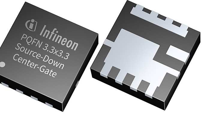
pqfn sd cg
The new generation of OptiMOS™ Source-Down (SD) power MOSFETs from Infineon come in a PQFN 3.3 x 3.3 mm2 package and a wide voltage class ranging from 25 V up to 100 V. The package enables a reduction in RDS(on) by up to 30 percent compared to the state of the art Drain-Down package. Additionally, the heat is dissipated directly into the PCB through a thermal pad instead of over the bond wire or the copper clip. This improves the thermal resistance RthJC by more than 20 percent, from 1.8 K/W down to 1.4 K/W.
JPEG
2126x1110 px
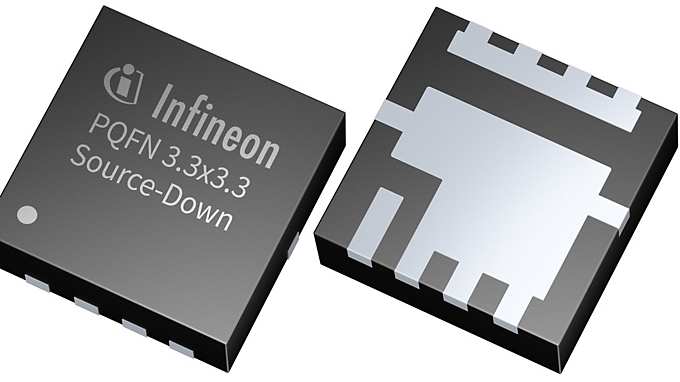
pqfn sd combi
The new generation of OptiMOS™ Source-Down (SD) power MOSFETs from Infineon come in a PQFN 3.3 x 3.3 mm2 package and a wide voltage class ranging from 25 V up to 100 V. The package enables a reduction in RDS(on) by up to 30 percent compared to the state of the art Drain-Down package. Additionally, the heat is dissipated directly into the PCB through a thermal pad instead of over the bond wire or the copper clip. This improves the thermal resistance RthJC by more than 20 percent, from 1.8 K/W down to 1.4 K/W.
JPEG
2126x1151 px
Information Number : INFPSS202201-041j