ThinPAK 5x6
The leadless SMD package for CoolMOS™ superjunction (SJ) MOSFET
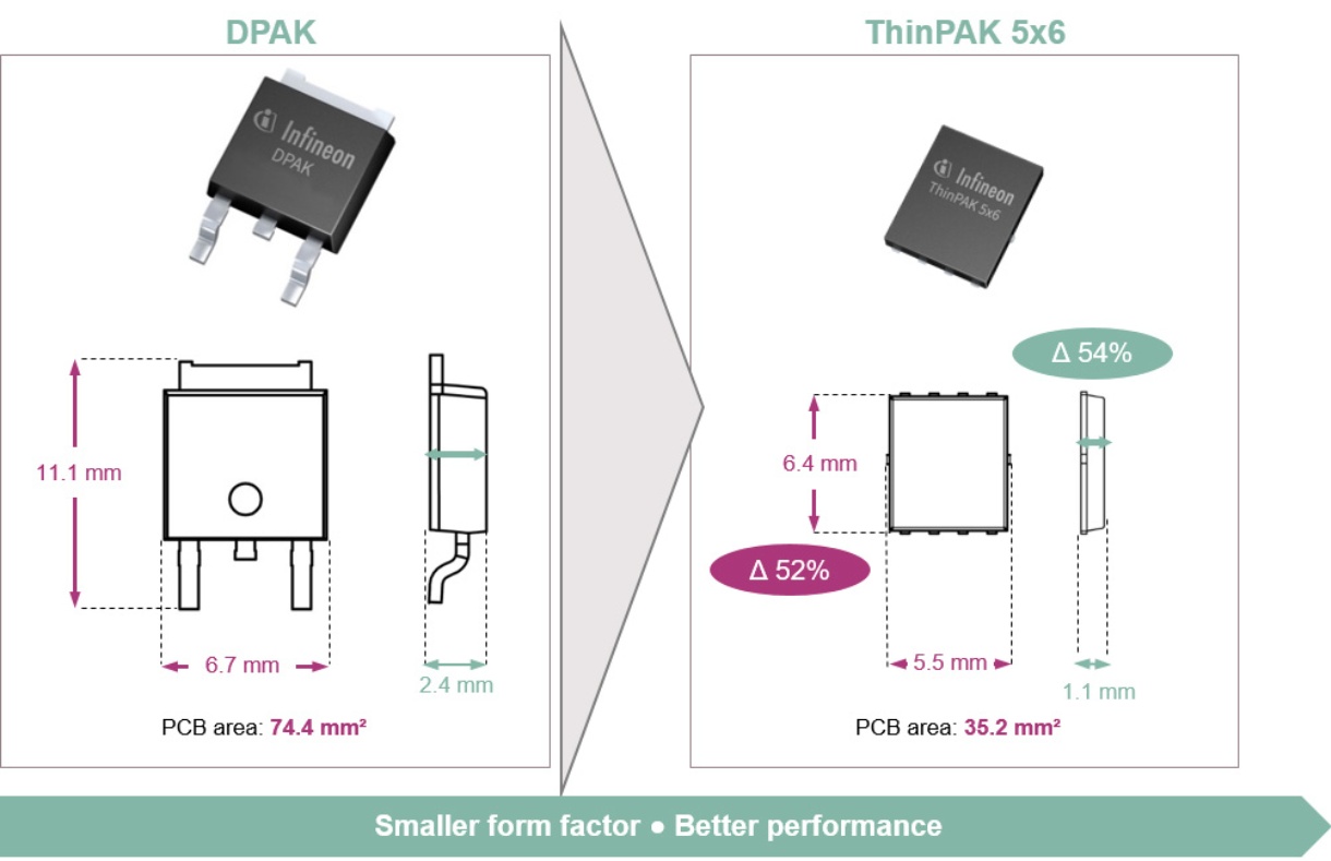
The ThinPAK 5x6 package is a leadless SMD package especially designed for high voltage MOSFETs. This package has a very small footprint of 5x6mm² and a very low profile with only 1mm height. The significantly smaller package size in combination with its benchmark low parasitics inductances can be used as a new and effective way to decrease system solution size in power- density driven designs.
The ThinPAK 5x6 package is characterized by a very low source inductance 1.6nH, as well as a similar thermal performance as DPAK. The package hence enables faster and thus more efficient switching of power MOSFETs and is easier to handle in terms of switching behavior and EMI.
The CoolMOS™ 7 families come in an improved version of this package, offering a 4-pin Kelvin source connection and hence improved signal integrity and efficiency.
Features
- 4-pin Kelvin source connection (for CoolMOS™ 7 families)
- Small footprint (5x6mm²)
- Low profile (1mm)
- Low parasitic inductance
- RoHS compliant
- Halogen-free mold compound
Benefits
- Enabling improved signal integrity and improved efficiency
- 54 % less board space consumption over DPAK
- 52 % reduced package height compared to DPAK package
- Increased power density
- Short commutation loop
- Easy-to-use products
- Environmentally friendly