インフィニオンテクノロジーズがドレスデンに300mmウェーハ対応の新プラントを建設
インフィニオンテクノロジーズは、ドレスデン工場に新しい300mmプラント(モジュール)を開設することを発表しました。総投資額は今後3年間で10億ユーロ(概略1,000億円)以 上にのぼると見込まれます。この計画はドレスデンに約1,100名分の職場を創出します。
建設活動は、インフィニオンテクノロジーズSC300社(Infineon Technologies SC300 GmbH & Co. KG)によって運営されます。同社には、ザ クセン州政府と、M+Wツァンダー社(半導体プラントの計画と建設の専門会社)が参加することになっています。詳細は、起工式が行われる5月末に発表の予定です。ド レスデンにおけるモトローラ社との生産技術共同開発は将来、この新プラントで行う予定です。インフィニオンは、300mm技術を梃子として、業界全般よりも早期に生産性向上を達成できると期待しています。
インフィニオンテクノロジーズの社長兼最高経営責任者ウルリッヒ・シューマッハは「300mm技術を先導することによって、半導体生産で大幅なコスト削減を達成し、長 期的な競争力を高められると期待しています。ドレスデン工場は、インフィニオンの国際工場群(ファブクラスタ)の基準拠点としての役割を果たしてきました。今後さらに、次 世代チップを効率的に生産するためのすぐれた基盤を提供するでしょう」と、話しました。
新しい300mmプラントは、既存プラントに隣接して建設されます。新プラントは、インフィニオンにおける約1,100名分の新しい職場と、地域の納入会社の新しい仕事を創出することになります。
300mm技術の開発は1998年1月から、モトローラ社との合弁会社において、ドイツ連邦教育技術省(BMBF)とザクセン州の出資を受けて行われてきました。両 社は1999年2月にドレスデンのパイロットプラントで300mmウェーハ上に最初の機能チップを実現しました。1999年6月には、3 00mmウェーハの良品チップ数が200mmウェーハの限界数を突破しました。1999年10月からインフィニオンは300mmウェーハを適用した64MビットDRAMを客先へ納入しています。インフィニオンは、 300mmプロセス技術を適用することによってチップコストを大幅に削減することを目指し、300mmによる量産を半導体生産における競争力を高めるための重要な要素と位置づけています。新 技術を適用したこの大型ウェーバでは、200mm技術と比較して、約2.5倍の数量のチップを生産できます。
インフィニオンの現在のドレスデン工場は、欧州における最先端チップ生産プラントのひとつに数えられます。現在、約2,800名の従業員がこのハイテクプラントで半導体デバイスを生産しています。こ のプラントは1994年6月に建設が開始され、現在では国際的にも最先端設備のひとつに数えられます。インフィニオンはこの工場から、先進メモリチップや高価値ロジックチップを世界各地へ供給しています。
インフィニオンについて
インフィニオンテクノロジーズ(Infineon Technologies AG)は、ドイツのミュンヘンに本社を置き、自 動車および産業分野や有線通信市場のアプリケーションへ向けた半導体およびシステムソリューション、セキュア・モバイル・ソリューション、メモリ製品などを供給しています。米国ではカリフォルニア州サンノゼ、ア ジア太平洋地域ではシンガポール、そして日本では東京を拠点として活動しています。2003会計年度(9月決算)の売上高は61億5,000万ユーロ、2003年9月末の従業員数は約32,300名でした。イ ンフィニオンは、フランクフルトとニューヨークの証券取引所に株式上場されています。
Information Number
INFXX200003.052
Press Photos
-
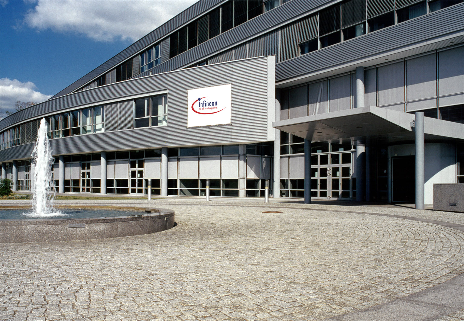
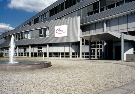 Infineon Technologies Dresden, one of the most modern chip factories in Europe, developed since its foundation in 1994 into a reference location for technology development within Infineon's worldwide "fab cluster". Currently about 2,800 employees are working in the fab, supported by another 2,000 external service-providers. Besides 64Mbit and 256Mbit memory components, embedded DRAMs and logic components on 200mm wafers are also manufactured. The 300mm technology will be implemented in a new module at the existing location. The picture shows the front view of the administration building with the main entrance and the communal area.Press Picture
JPG | 550 kb | 1535 x 1063 px
-
 Dr. Ulrich Schumacher President and CEO, Infineon Technologies AGPress Picture
JPG | 753 kb | 1063 x 1535 px
-
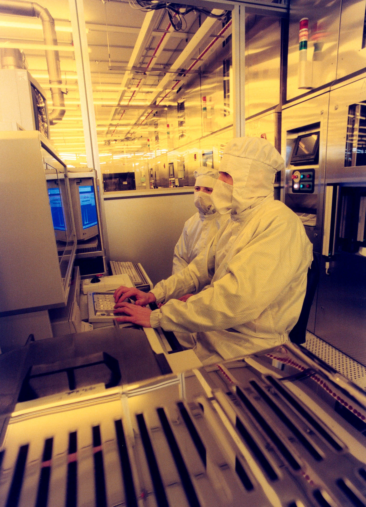
 Infineon Technologies Dresden, one of the most modern chip factories in Europe, developed since its foundation in 1994 into a reference location for technology development within Infineon's worldwide "fab cluster". Currently about 2,800 employees are working in the fab, supported by another 2,000 external service-providers. Besides 64Mbit and 256Mbit memory components, embedded DRAMs and logic components on 200mm wafers are also manufactured. The 300mm technology will be implemented in a new module at the existing location. The picture shows a working environment in the clean room (class 1) located in the manufacturing module 1. Using the scanning electron microscope, defects that have been discovered are classified directly on the production line. This method enables to trace the faults' cause and to take the appropriate countermeasures.Press Picture
JPG | 567 kb | 1535 x 2126 px