The making of a chip – from sand to semiconductor
Watch our new video and learn, how semiconductors – building blocks of a modern society - are made
Microelectronics usually is hidden to society – however, it is a constant companion in our daily lives. It tremendously contributes to the ongoing development and digitization of our world. But what is actually behind this technology?
It all starts with sand - but that is not all. The production of semiconductors is a very complex process. Starting with the raw material sand, many further manufacturing steps need to be completed until the end product is finished.
(duration: approx. 15 minutes)

Infineon Technologies is a world leader in semiconductor solutions that make life easier, safer and greener. Around the globe, teams of research and development experts are working on innovative answers to the global challenges of our time, addressing issues such as rapid population growth, the rise of megacities and the increasing scarcity of natural resources. Microelectronics are the key to supplying the world’s expanding population with energy, meeting demands for higher living standards and minimizing our impact on the environment. Microelectronics are also paving the way for smart mobility concepts, efficient energy management and the secured storage and transmission of data. Whether we are aware of it or not, countless everyday experiences and transactions are controlled by highly sophisticated microelectronic systems. These small, almost invisible microchips are already an integral part of our lives.
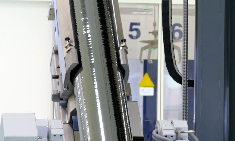
All chips start out with a very simple raw material: sand. Complex chemical and physical processes are required to create out of the sand an pure monocrystalline silicon ingot, called a boule, with only one impurity atom for every ten million silicon atoms. Extremely thin wafers are then cut from the silicon boules using a special sawing technique. These wafers are the basic building blocks for subsequent chip production. They are fabricated in a range of different diameters. The most common sizes are 150, 200 and 300 mm. Wafers with large diameters offer more space for chips. Silicon is a semiconductor. This means that it can conduct electricity and also act as an insulator. To allow it to become conductive, small quantities of specific atoms are added as impurities to the wafer. These impurity atoms must have a number of outer electrons that is either one more or one less than that of silicon. Depending on the number of outer electrons the material gets p-conductive or n-conductive. Transistors are built on the p- and n-conductive layers that exist in a doped wafer. Transistors are the smallest control units in microchips. Their job is to control electric voltages and currents and they are by far the most important components of electronic circuits. But how are these layers created on a wafer?

The process to manufacture chips from a wafer starts with the layout and design phase. Highly complex chips are made up of billions of integrated and connected transistors, enabling sophisticated circuits such as microcontrollers and crypto chips to be built on a semiconductor surface measuring just a few square millimeters in size. The sheer number of components calls for an in-depth design process. This entails defining the chip’s functions, simulating its technical and physical properties, testing its functionality and working out the individual transistor connections.

First of all, the surface of the wafer is oxidized in a high-temperature furnace operating at approximately one thousand degrees Celsius to create a non-conductive layer. Then, a photo resist material is uniformly distributed on this non-conductive layer using centrifugal force. This coating process creates a light-sensitive layer. The wafer is then exposed to light through the photomask in special exposure machines known as steppers. The exposed area of the chip pattern is developed, revealing the layer of oxide below. The unexposed part remains as is, protecting the layer of oxide. After this, the exposed layer of oxide is etched off in the areas that have been developed using wet or plasma etching. Then, photoresist is applied again, and the wafer is exposed to light through the mask. The exposed photoresist is stripped again.
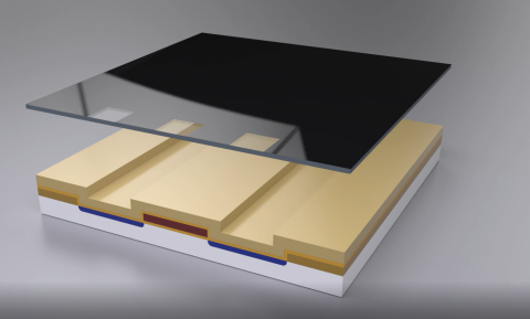
The next step is the doping process, where impurity atoms are introduced into the exposed silicon. An ion implanter is used to shoot impurity atoms into the silicon. This changes the conductivity of the exposed silicon by fractions of a micrometer. After the photoresist residue has been stripped, another oxide layer is applied. The wafer undergoes another cycle of applying photoresist, exposure through the mask and stripping. Contact holes are etched to provide access to the conductive layers, enabling the contacts and interconnections to be integrated in the wafer. Once again, the photoresist and mask are applied. To give the insulation layer above the interconnections the smooth finish it requires, a chemical-mechanical process is used to polish away excess material with micrometer accuracy. These individual steps may be repeated multiple times in the fabrication process until the integrated circuit is complete. Depending on the size and type of chip, the wafer will now contain anything from several dozen to thousands of chips.
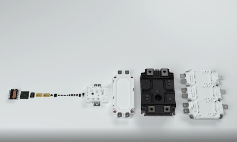
The final stage of fabrication is assembly. Here, the individual chips are placed in a package and terminals are attached. The result is a finished semiconductor device, which can be mounted on circuit boards using different types of terminals. Over a thousand connection contacts can be realized. The high levels of precision and quality are essential at every stage of the workflow – from the production of silicon boules through cleanroom fabrication to quality control – in order to deliver these tiny building blocks that have such a big impact on our lives – today and in the future.