Infineon introduces new ThinPAK 8x8 leadless SMD package for HV Power MOSFETs designed to enable higher power density solutions
Neubiberg, Germany – May 3, 2010 – Infineon Technologies today introduces the ThinPAK 8x8, a new leadless SMD package for HV MOSFETs. The new package has a very small footprint of only 64mm² (vs. 150mm² for the D2PAK) and a very low profile with only 1mm height (vs. 4.4mm for the D2PAK). The significantly smaller package size, combined with benchmark low parasitic inductances, provides designers with a new and effective way to decrease system solution size in power density driven designs.
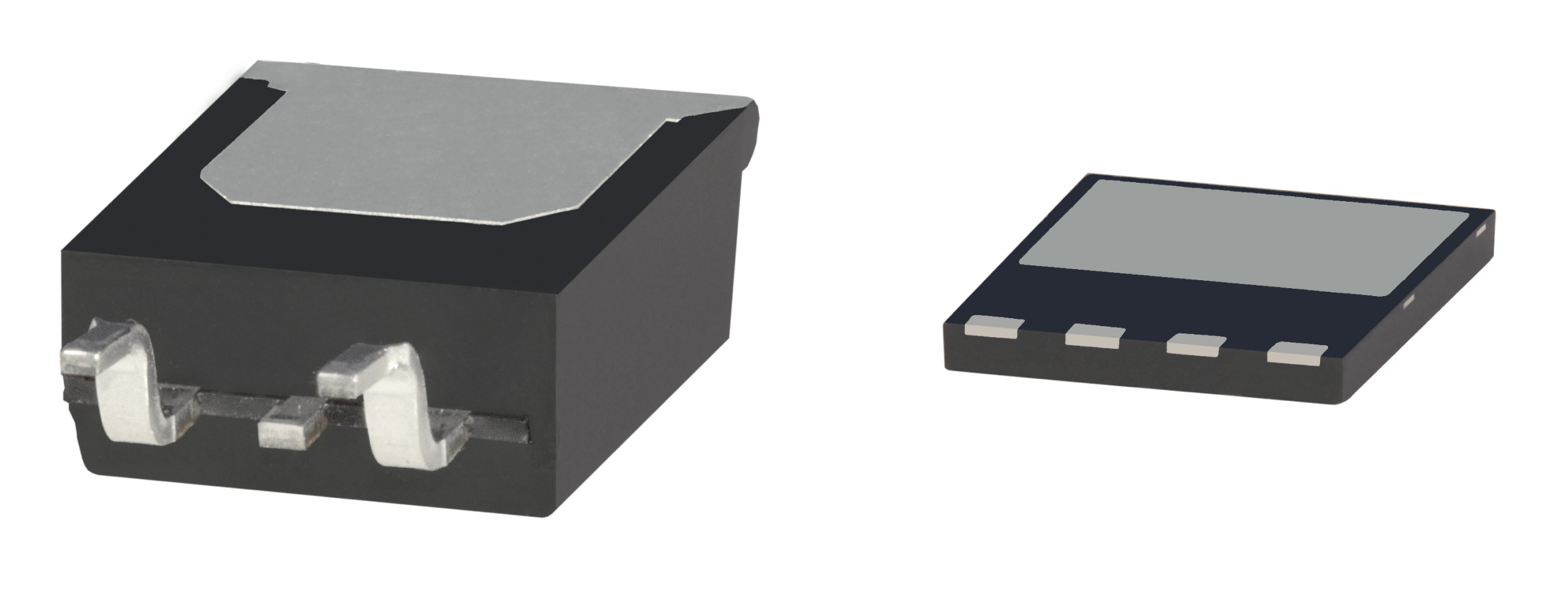
The new 1 mm-high surface-mount package houses the industry-standard TO-220 die size within a leadless outline measuring only 8x8 mm and features an exposed metal drain pad for efficient removal of internally generated heat. Its low profile will enable designers to achieve slimmer power supply enclosures enabling compact and stylish new products for today’s markets. This new standard is available from two companies: Infineon and ST will introduce MOSFETs using this innovative package, which is named ThinPAK 8x8 by Infineon and PowerFLAT™ 8x8 HV by ST, therefore providing customers with a high-quality alternative source.
“This type of package sets a new market standard for leadless SMD packages for HV MOSFETs, and is being introduced today in co-operation with STMicroelectronics,” said Jan-Willem Reynaerts, Product Line Manager HVMOS Power Discretes at Infineon Technologies. ”Silicon technologies like CoolMOS™ have reached such an advanced stage of fast and efficient switching, that the standard traditional through-hole packages more and more have become the limiting factor in getting to the next level of energy efficiency and power density.”
The ThinPAK 8x8 package is characterized by a very low source inductance of only 2nH (vs. 6nH for the D2PAK), a separate driver source connection for clean gate signals, as well as a thermal performance similar to the D2PAK. As a result, the ThinPAK 8x8 package enables faster and thus more efficient switching of Power MOSFETs and is also easier to handle in terms of switching behavior and EMI.
Infineon will initially offer three 600V CoolMOS™ devices in the new package: 199 mOhm (IPL60R199CP), 299 mOhm (IPL60R299CP) and 385 mOhm (IPL60R385CP).
Availability
Qualification samples of the new devices in ThinPAK 8x8 packages are now available, with production volumes available against forecast within standard lead times.
Further information
Infineon presents the new ThinPAK 8x8 package and other innovations at its booth (hall 12, booth 428) at PCIM, May 4-6, 2010 in Nuremberg, Germany.
Additional information on the ThinPAK 8x8 package and the Infineon portfolio of MOSFETs is available at www.infineon.com/thinpak8x8
About Infineon
Infineon Technologies AG, Neubiberg, Germany, offers semiconductor and system solutions addressing three central challenges to modern society: energy efficiency, communications, and security. In the 2009 fiscal year (ending September), the company reported sales of Euro 3.03 billion with approximately 25,650 employees worldwide. With a global presence, Infineon operates through its subsidiaries in the U.S. from Milpitas, CA, in the Asia-Pacific region from Singapore, and in Japan from Tokyo. Infineon is listed on the Frankfurt Stock Exchange (ticker symbol: IFX) and in the USA on the over-the-counter market OTCQX International Premier (ticker symbol: IFNNY).
Information Number
INFIMM201005.044
Press Photos
-
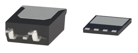 The new ThinPAK 8x8 leadless SMP package has a very small footprint of only 64mm² (vs. 150mm² for the D2PAK) and a very low profile with only 1mm height (vs. 4.4mm for the D2PAK).D2PAK_ThinPAK
JPG | 440 kb | 2555 x 982 px