Infineon Announces Shipment of World´s Smallest 512 Megabit DDR2 Memory Components to Intel; Infineon´s DDR2 Memory Technology Successfully Boots with Intel Corporation´s Next Generation "Lindenhurst" Dual Processor Server Chipset
Munich/Germany and San Jose/USA, September 17, 2003 Infineon Technologies (FSE/NYSE: IFX) today announced at the Intel Developer Forum that its initial 512 Megabit (Mb) DDR2 (second-generation Double-Data-Rate) SDRAM is successfully booting and is under evaluation with Intels next generation dual processor server chipset code name Lindenhurst. Infineon´s 512 Megabit x8 DDR2 SDRAM devices are under evaluation by Intel and compliant with JEDEC's DDR2 specification.
Infineons DDR components are designed for next generation, high-performance main memory in Server, PC and Workstation applications. The new 512 Mb DDR2 components are fabricated using Infineons advanced 110 nanometer (nm) CMOS process technology; which results in lowest power consumption and the smallest chip size in the industry for this density.
The initial Infineon DDR2 components operate at per pin data rates of 400 Mbps (megabits per second) and 533 Mbps. Components and memory modules operating at higher speeds are already in preparation for systems using DDR2 main memory beginning in 2004. Infineons roadmap for DDR2 also includes 256 Mb and 1 Gigabit components in 2004.
Infineons DDR2 memory technology will enable Intels desktop, server and mobile platforms to achieve higher performance, lower power and increased capacity in 2004, said Pete MacWilliams, Senior Fellow, Intel Corporation. I expect DDR2 technology to be the key memory architecture for several years.
Memory modules based on DDR2-533 will achieve data rates of 4.3 GigaBytes per second, providing systems with truly remarkable performance using a mainstream, industry standard memory architecture, said Bernd Lienhard, Vice President Memory Products at Infineon Technologies North America. As the memory supplier leading the industrys transition to cost-effective, high-volume production on 300 mm wafers, we are proud to join Intel in offering computer users leading edge technology for the next level of systems design.
Infineons JEDEC compliant 512Mb DDR2 chips are configured as quad-bank DRAMs, will be available in x4, x8 and x 16 organizations, and are offered in FinePitch Ball Grid Array (FBGA) packages. Additional features of the new memory include a pre-fetch size of 4 bits, differential strobe and variable data-output impedance adjustment.
About Infineon
Infineon Technologies AG, Munich, Germany, offers semiconductor and system solutions for the automotive and industrial sectors, for applications in the wired communications markets, secure mobile solutions as well as memory products. With a global presence, Infineon operates in the US from San Jose, CA, in the Asia-Pacific region from Singapore and in Japan from Tokyo. In the fiscal year 2002 (ending September), the company achieved sales of Euro 5.21 billion with about 30,400 employees worldwide. Infineon is listed on the DAX index of the Frankfurt Stock Exchange and on the New York Stock Exchange (ticker symbol: IFX). Further information is available at www.infineon.com.
Information Number
INFMP200309-121
Press Photos
-
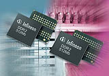
 The world´s smallest 512-Mbit DDR2 Memory Component by Infineon Technologies boots successfully with Intel´s new "Lindenhurst" Dual Processor Server Chipset. New 512 Mb DDR2 components are fabricated using Infineon´s advanced 110 nanometer CMOS process technology.512-Mbit DDR2
JPG | 362 kb | 1535 x 1063 px
512-Mbit DDR2JPG | 11 kb | 160 x 111 px