Infineon Technologies Demonstrates that Further Shrinking of Today's State-of-the-Art Chip Wiring Technique Will Result in Wires Meeting Electrical Reliability Requirements for Chip Manufacturing Into Next Decade
Munich/Germany, May 31, 2002 - Infineon Technologies (FSE/NYSE: IFX) today announces that its Munich Research Labs have demonstrated, by extending present integrated circuit wiring to smaller feature sizes, that the requirements regarding electrical reliability will be met by wiring schemes in future chip generations extending to the 2010 timeframe.
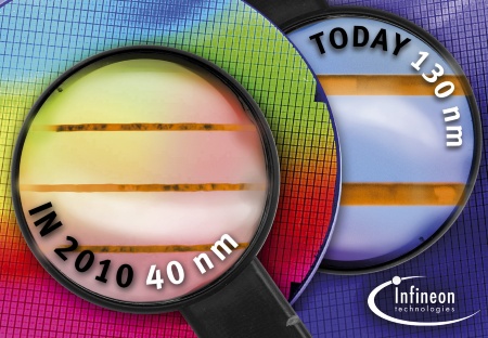
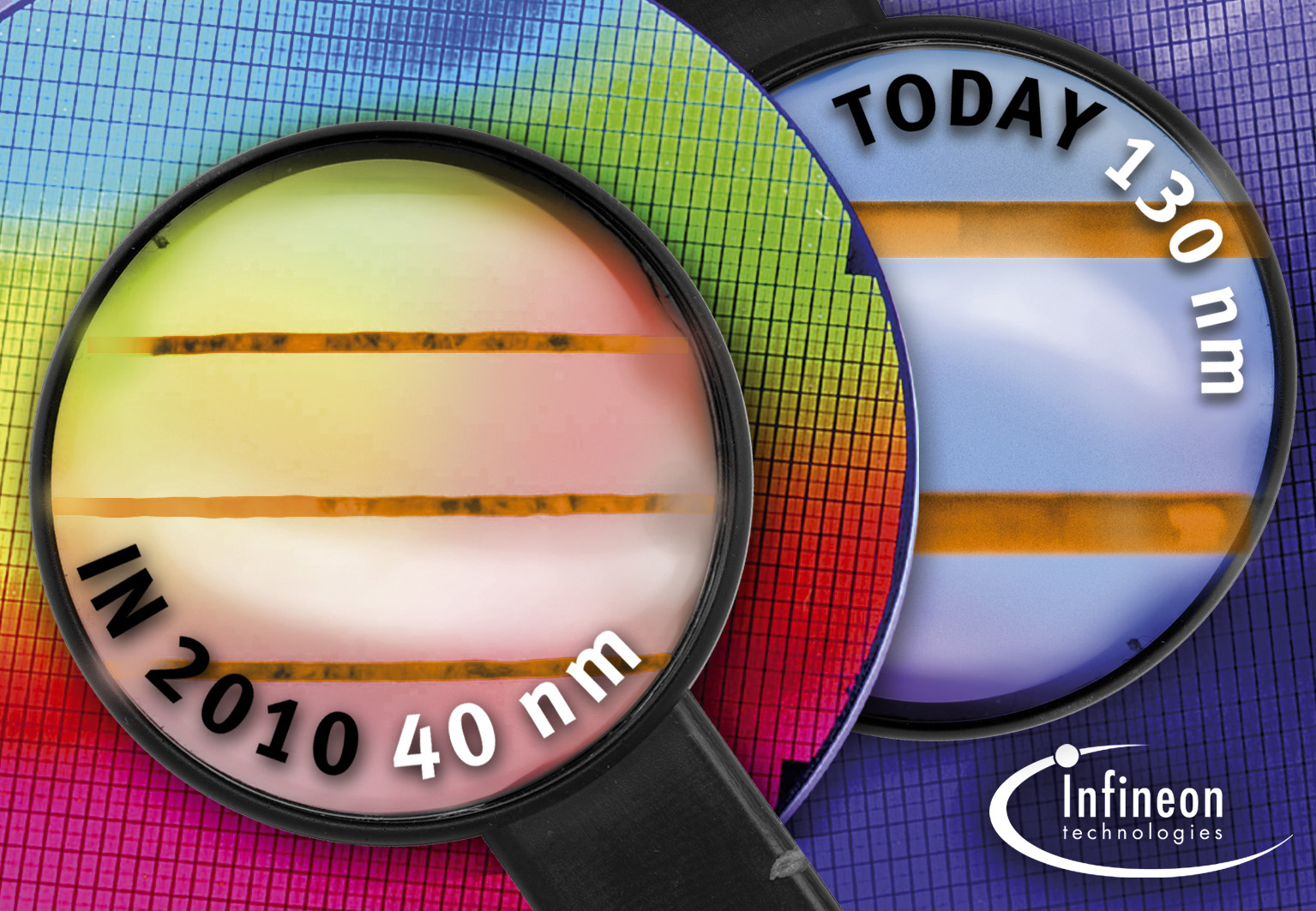
Infineon researchers have successfully performed an electrical assessment of sub-70nm metal lines down to 40nm line widths, embedded in grooves of a dielectric film used for electrical isolation. Metal lines as narrow as 55nm will be used for the shortest electrical connections between the transistors in the generation of integrated
circuits which is expected to be in production in 2010.
The obtained maximum current densities in these copper lines were in the 80-100 Million Ampere/cm2 regime. These current densities are exceeding those known from today's most advanced technologies by a factor of 2 to 5. These extremely high current carrying capabilities are mainly attributed to very efficient heat transfer to the intermetal dielectric surrounding the metal lines. The heat transfer to the intermetal dielectric was achieved by the favorable ratio of surface to cross-sectional area of these metal lines. The wires investigated had profile heights exceeding the wire widths.
"With the evaluation of the test results we have proven that the manufacture of high-reliability ultra-thin connections is not an insurmountable technical problem in the continued process of making chips smaller," said Dr. Sönke Mehrgardt, member of the board and chief technology officer of Infineon Technologies AG. "Todays connection technology can thus in principle be applied for future chip generations as described in the International Technology Roadmap for Semiconductors (ITRS), which at present extends to the year 2016."
Supreme electromigration resistance is a key requirement for chip metallization schemes. High current densities are the driving force for material transport in metallic wires which, in turn, degrades reliability and makes wires prone to failure. Intrinsically high inertness against electromigration is therefore a key criterion for an assessment of the quality of chip wiring.
In a thorough investigation of electromigration resistance, a mean time to failure of sub-70nm copper lines of 80-90 years was obtained, a value comparable with that obtained for today's products with 180nm critical dimensions. The assessment of electromigration resistance was performed with the stringent standard evaluation methods used for the metallization schemes in today's products.
Lithography tools needed for the fabrication of chip generations in the 2010-13 timeframe do not yet exist. Infineon overcame this issue by using a spacer technique to narrow the mask openings defined by today's manufacturing lithography for pattern transfer into the dielectric film. This allows the production of structures with lateral dimensions far below the feature sizes that can be realized with today's most advanced lithography manufacturing equipment.
The copper wires investigated were fabricated with the damascene technique, the state-of-the-art approach in the semiconductor industry to realize advanced chip metallization. In this technique, grooves and holes are filled by deposition of metal followed by a complete removal of all metal covering the filled structures by chemical mechanical polishing. The technique is named after the way ornaments were once applied in damascene swords.
The silicon wafers used for the electrical assessment of the embedded copper lines were processed with today's standard semiconductor manufacturing equipment and processes developed for 250nm feature sizes in the cleanroom of International Sematech, Austin, TX, a consortium of the world's leading semiconductor manufacturers.
About Infineon
Infineon Technologies AG, Munich, Germany, offers semiconductor and system solutions for applications in the wired and wireless communications markets, for security systems and smartcards, for the automotive and industrial sectors, as well as memory products. With a global presence, Infineon operates in the US from San Jose, CA, in the Asia-Pacific region from Singapore and in Japan from Tokyo. In the fiscal year 2001 (ending September), the company achieved sales of Euro 5.67 billion with about 33,800 employees worldwide. Infineon is listed on the DAX index of the Frankfurt Stock Exchange and on the New York Stock Exchange (ticker symbol: IFX). Further information is available at www.infineon.com.
Information Number
INFCPR200205.097 e
Press Photos
-
 Infineon Technologies Demonstrates that Further Shrinking of Today's State-of-the-Art Chip Wiring Technique Will Result in Wires Meeting Electrical Reliability Requirements for Chip Manufacturing Into Next DecadePress Picture
JPG | 488 kb | 1535 x 1063 px