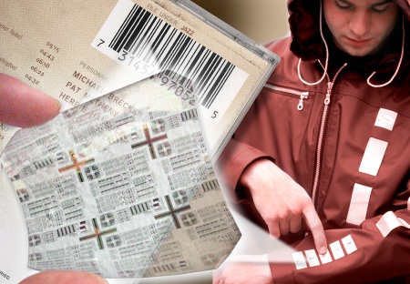
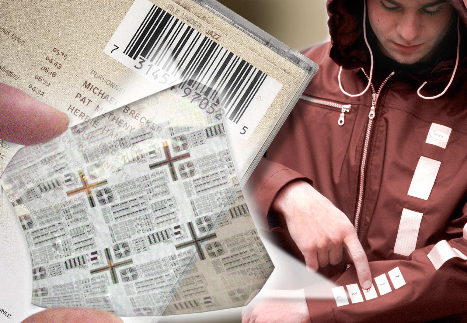
Infineon Technologies has developed Polymer chips with excellent electrical characteristics and optimised them for cost-effective manufacturing
Munich, November 12, 2002 Infineon Technologies has announced today that the companys research laboratories have developed and manufactured organic transistor-based electronic circuits on various substrates. These circuits have achieved performance capability levels that were previously unattainable. The thin-film transistors (TFTs) manufactured by Infineon use organic semiconducting molecules as the active layer and achieve charge carrier mobilities in excess of 1 cm²/ Vs. The high electrical performance capability that has been achieved and the manufacturing method upon which it is based, which is geared toward low-cost mass production, meet the essential criteria for future polymer electronic products in applications that demand the large-scale manufacture of ultra-low-cost electronic implementations.
With regard to integration density and clock frequency, polymer electronics may not be a direct alternative to silicon-based integration, but it has the major benefits of extremely low-cost manufacture and a high degree of flexibility. While the manufacture of integrated circuits using silicon or other crystalline semiconductors requires a large number of sequential processes with expensive equipment, and is therefore tedious and relatively expensive, polymer electronics can be manufactured rapidly, at low cost and in large quantities. Among the applications envisioned for polymer electronics are wireless tags (RF ident tags), flat panel displays, large sensor arrays and biochemical sensors.
Since all the materials required to manufacture electronic circuits (i.e. semiconductors, insulators and conductors) are available in the form of polymers, it is in principle possible to dissolve all these materials in suitable solvents and apply them subsequently to the substrate from solution to achieve the required electronic functionality. Organic insulators and organic conductors have in fact been successfully processed from solution by the Infineon researchers. Organic semiconductors, on the other hand, are far more difficult to dissolve, at least in environmentally friendly solvents, meaning that toxic chlorinated solvents have to be used for processing. Infineon therefore uses small organic molecules that can be applied from the gas phase without using solvents and which also tend to have better performance compared with polymeric semiconductors. Another advantage of working with small molecules is that they can be purified with relative ease by sublimation, whereas the purification of polymers requires elaborated and expensive chromatographic procedures.
The Infineon researchers have developed a broad portfolio of processes that can be combined in a variety of ways and can be used to manufacture high-quality organic transistors and circuits using conventional deposition processes and photo-lithographic patterning techniques. The Infineon scientists have also succeeded in using microcontact printing (a relief printing method similar to flexographic printing) to pattern transistors and circuits, with feature size and electrical performance similar to those of transistors and circuits fabricated using by photolithography.
The latest research results at Infineon show that plastic-based integrated circuits can be a potential addition to silicon chips in high volume and extremely cost-critical applications, said Dr. Soenke Mehrgardt, CTO of Infineon Technologies. Possible applications for low-cost polymer ICs are RF ID tags as an alternative to barcodes or for use in the wearable electronics area.
Like their silicon pendants, organic transistors consist of several layers: substrate, gate electrode, gate insulator, source and drain contacts, organic semiconductors (e.g. pentacene or substituted oligothiophenes), and a protective passivation layer. Infineon develops both hybrid organic/inorganic structures as well as all-polymer chips. Organic semiconductors often show their highest charge carrier mobility when deposited on inorganic gate insulators, such as silicon dioxide. Charge carrier mobilities, greater than 2 cm²/Vs have been achieved with inorganic gate insulators in the past. However, the deposition of high quality inorganic insulator layers requires time-consuming vacuum processes. In order to make large-scale manufacturing cheaper it is highly desirable to replace the inorganic insulators with polymer insulators that are easier to process.
The main goals of the Infineon researchers were to substitute silicon dioxide with a polymer gate insulator, and to manufacture transistors and circuits on a wide range of substrates, including low-cost, flexible plastic film. In order to achieve these goals, formulations and processes have been developed for the fabrication of high-mobility organic TFTs using polyvinyl phenol as the organic gate insulator and pentacene as the organic semiconductor. In this case, a charge carrier mobility of 3 cm²/Vs was measured using thermally evaporated gold layers for the source and drain contacts; this is the highest mobility that has ever been measured for organic TFTs. Using these pentacene TFTs the Infineon researchers succeeded in manufacturing digital circuits with a maximum clock frequency of 45 kHz (for circuits on flexible plastic substrates) and 65 kHz (for circuits on rigid glass substrates). Higher clock frequencies can be obtained by reducing the critical TFT dimensions from currently 5 µm to 1 µm, but a minimum feature size below about 5 µm is unrealistic for low-cost, flexible-substrate mass production.
Another goal the Infineon team accomplished is the fabricaton of transistors and circuits that are made entirely of organic materials, i.e. without the use of inorganic insulators and inorganic metals. This was achieved by using the synthetic metal PEDOT:PSS, and the charge carrier mobility of 0.3 cm²/Vs measured for these devices is a record for TFTs with organic source and drain contacts.
The Infineon researchers are not only involved in technology development, but also design circuits optimized for the special requirements of polymer electronics. For example, this includes the implementation of circuit designs with a high degree of tolerance with regard to parameter variability, which is unavoidable in low-cost mass production. Components that cannot be manufactured or are difficult to manufacture using organic materials such as high-quality diodes, will be implemented using equivalent transistor circuits.
About Infineon
Infineon Technologies AG, Munich, Germany, offers semiconductor and system solutions for the automotive and industrial sectors, for applications in the wired communications markets, secure mobile solutions as well as memory products. With a global presence, Infineon operates in the US from San Jose, CA, in the Asia-Pacific region from Singapore and in Japan from Tokyo. In the fiscal year 2002 (ending September), the company achieved sales of Euro 5.21 billion with about 30,400 employees worldwide. Infineon is listed on the DAX index of the Frankfurt Stock Exchange and on the New York Stock Exchange (ticker symbol: IFX). Further information is available at www.infineon.com
Information Number
INFCPR200211.016e
Press Photos
-
 Infineon Technologies has developed Polymer chips with excellent electrical characteristics and optimised them for cost-effective manufacturingPress Picture
JPG | 695 kb | 1535 x 1063 px