Pioneering 300: Infineon launches volume production of semiconductors on 300 mm wafers - Putting smallest chips on biggest wafers cuts production costs up to one-half
Dresden, Germany - December 12, 2001. - Infineon Technologies (FSE/NYSE: IFX) today officially commenced volume production of semiconductors processed on silicon wafers with a diameter of 300 mm (12 inch). As the first chip manufacturer in the world to begin volume production using 300 mm wafers, compared to the current 200 mm (8 inch) technology used by all other manufacturers, Infineon extends its technology and production cost leadership position in the semiconductor industry. The increased number of chips that can fit on the surface of a 300 mm wafer - around 2.5 times as many as on the 200 mm wafer yields production cost advantages of up to 30 percent. With a concurrent switch to smaller device geometries (0.14 microns) Infineon expects to ultimately reduce its production costs by a further 30 percent. In comparison with 200 mm wafers processed in 0.17-micron technology, Infineon will approximately halve its production costs for DRAM chips at the Dresden facility. Infineon also anticipates that the demand for DRAM memory (measured in total bits) in 2002 will increase by 50 percent compared with 2001.
If you want to prevail in tomorrows semiconductor market, you have to be willing to make counter-cyclical investments today, stated Dr. Ulrich Schumacher, CEO of Infineon Technologies, at an international press briefing today in Dresden. Right here in this city, we invested in a technology that will allow us to produce the smallest possible chips on the largest possible wafers for the lowest possible costs. This will allow us to expand sharply our recognized cost leadership within the industry. The corresponding jump in productivity gives us a technology edge of more than 15 months on the competition, giving us unrivaled flexibility within our volatile market.
The beginning of volume production on 300 mm wafers means a new manufacturing dimension for ourselves and the semiconductor industry as a whole, said Dr. Andreas von Zitzewitz, board member and COO of Infineon Technologies. Weve established a new standard with our 300 mm technology. Infineon is clearly the trend-setter in this area. This superb accomplishment at our Dresden location is a further proof of the state of Saxonys capacity for technological innovation - over 80 percent of our Dresden team comes out of this area.
Currently, Infineon has around 4,300 employees at its Dresden facility. More than 800 are now engaged in 300 mm production, and any future capacity expansion would likely result in more headcount. Infineon has invested around Euro 1.1 billion in the 300 mm wafer production technology in Dresden. M+W Zander, internationally recognized specialists in planning and building semiconductor production facilities, have invested Euro 51 million in the project, and the exhibition company, Leipziger-Messe GmbH, has invested Euro 118 million in the 300 mm-production facility.
Initially, Infineon will bring approximately 11,000 wafers per month into the production cycle. Depending on the development of the worldwide semiconductor market, capacity can be increased to more than 16,000 wafer starts per month by the end of 2002. The maximum capacity of the 300 mm-production facility is around 25,000 wafer starts per month.
Infineon is launching its volume production at the 300 mm plant in Dresden by manufacturing 256 Mbit memory chips, a standard component for personal computers and servers. This DRAM is currently the industrys smallest 256 Mbit chip, containing almost 540 million electronic components (transistors and capacitors) on less than 64 mm². Infineon also is one of the first companies to deliver first samples of the next density generation, 512 Mbit SDRAMs, to strategic partners in the PC industry.
In semiconductor chip production, the usable surface of a silicon wafer measuring 300 mm in diameter exceeds that of a 200 mm wafer by a factor of about 2.5. The structures of the semiconductors produced in Dresden using 0.14 micron technology are around 30 per cent smaller than the previous generation measuring 0.17 microns.
Smaller structures and bigger wafer surfaces mean that Infineon can put approximately 3.5 times as many chips on a single wafer - a technological feat that translates into the worlds most competitive production cost position.
Infineons memory components give the company a uniquely broad spectrum of memory chips compared to competitors: including standard PC and server memory chips, extremely fast memory chips for use in network infrastructure systems, and products with especially low-power leakage for battery-powered computer and electronic appliances. Infineon also produces special memory chips for computer graphics systems and mobile telephones as well as Personal Digital Assistants.
Infineon ultimately will use 300 mm wafers also in its logic chip production. These chips are used in numerous applications, including mobile phones, chip cards, telecommunications and automotive and industrial electronics. To this end, UMCi, a joint venture of Infineon and UMC, is building a new facility in Singapore. By using similar technology to produce logic and DRAM memory chips, Infineon will be able to react even more flexible to future fluctuations in demand.
The Dresden plant is part of Infineons DRAM chip production cluster, which includes production facilities in Richmond, Virginia (USA), and ProMOS Technologies, a joint venture with Mosel Vitelic based in Hsinchu (Taiwan). At the Taiwan facility, the 300 mm and 0.14 micron technologies are just beginning to be set up, and production there could commence by early summer 2002. The Richmond plant is ready for installation of the new technology. Depending on market development, 300 mm production could be launched at that plant within a matter of months.
With almost 14 per cent of worlds market share, Infineon is currently number four in sales of DRAM memory chips worldwide. Sales of memory components in the last financial year amounted to Euro 1.59 billion, around 28 per cent of overall sales. Behind Communication Technology (Euro 2.35 billion, 42 per cent) and ahead of the Automotive & Industrial business group (Euro 1.1 billion, 19 per cent), the Memory Products business group was Infineons No. 2 sales engine last year.
About Infineon
Infineon Technologies AG, Munich, Germany, offers semiconductor and system solutions for applications in the wired and wireless communications markets, for security systems and smartcards, for the automotive and industrial sectors, as well as memory products. With a global presence, Infineon operates in the US from San Jose, CA, in the Asia-Pacific region from Singapore and in Japan from Tokyo. In the fiscal year 2001 (ending September), the company achieved sales of Euro 5.67 billion with about 33,800 employees worldwide. Infineon is listed on the DAX index of the Frankfurt Stock Exchange and on the New York Stock Exchange (ticker symbol: IFX). Further information is available at www.infineon.com.
Note:
The presentations to mark the beginning of volume production at the 300 mm facility, featuring CEO Dr. Ulrich Schumacher and COO Dr. Andreas von Zitzewitz, will be broadcast live on the Internet beginning at 1:30 p.m. CET. Journalists can view the broadcast at www.pioneering300.com. We recommend that you visit the above site early in case you need to download any extra software in order to view the presentation. A video of the presentation will subsequently be available at the same site.
Disclaimer:
This discussion includes forward-looking statements about our future business. These forward-looking statements include statements relating to future developments of the world semiconductor market, especially the market for memory products, Infineons future growth, the benefits of research and development alliances and activities, our planned levels of future investment in the expansion and modernization of our production capacity, the introduction of new technology at our facilities, the transitioning of our production processes to smaller structures, cost savings related to such transitioning and other initiatives, our successful development of technology based on industry standards, our ability to offer commercially viable products based on our technology, our ability to achieve our cost savings and growth targets. These forward-looking statements are subject to a number of uncertainties, including trends in demand and prices for semiconductors generally and for our products in particular, the success of our development efforts, both alone and with our partners, the success of our efforts to introduce new production processes at our facilities and the actions of our competitors, the availability of funds for planned expansion efforts, as well as the other factors mentioned herein. As a result, our actual results could differ materially from those contained in the forward-looking statements.
Infineon, the stylized Infineon Technologies design are trademarks and servicemarks of Infineon Technologies AG. All other trademarks are the property of their respective owners.
Press Photos
-
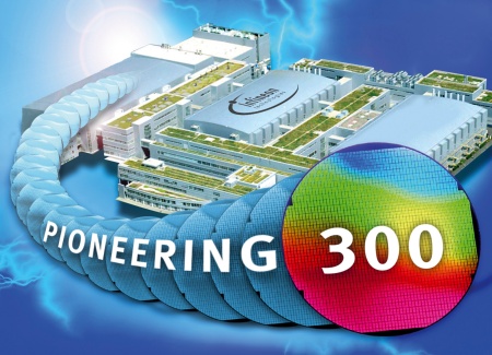 Pioneering 300: Infineon launches worlds' first 300mm line - The world's first semiconductor line offering ultra-small chips on 300mm wafers is now in volume production at the Infineon Technologies plant in Dresden.Press Photo
JPG | 1.12 mb | 2126 x 1535 px
Press PhotoJPG | 15 kb | 160 x 116 px