Small diameter with huge impact
All the milestones presented so far have one thing in common: the conviction of all those involved that you can only be successful in the long term if you dare to break new ground. This applies to groundbreaking developments from Linz and Graz just as it does to innovations in manufacturing technology.
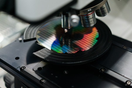
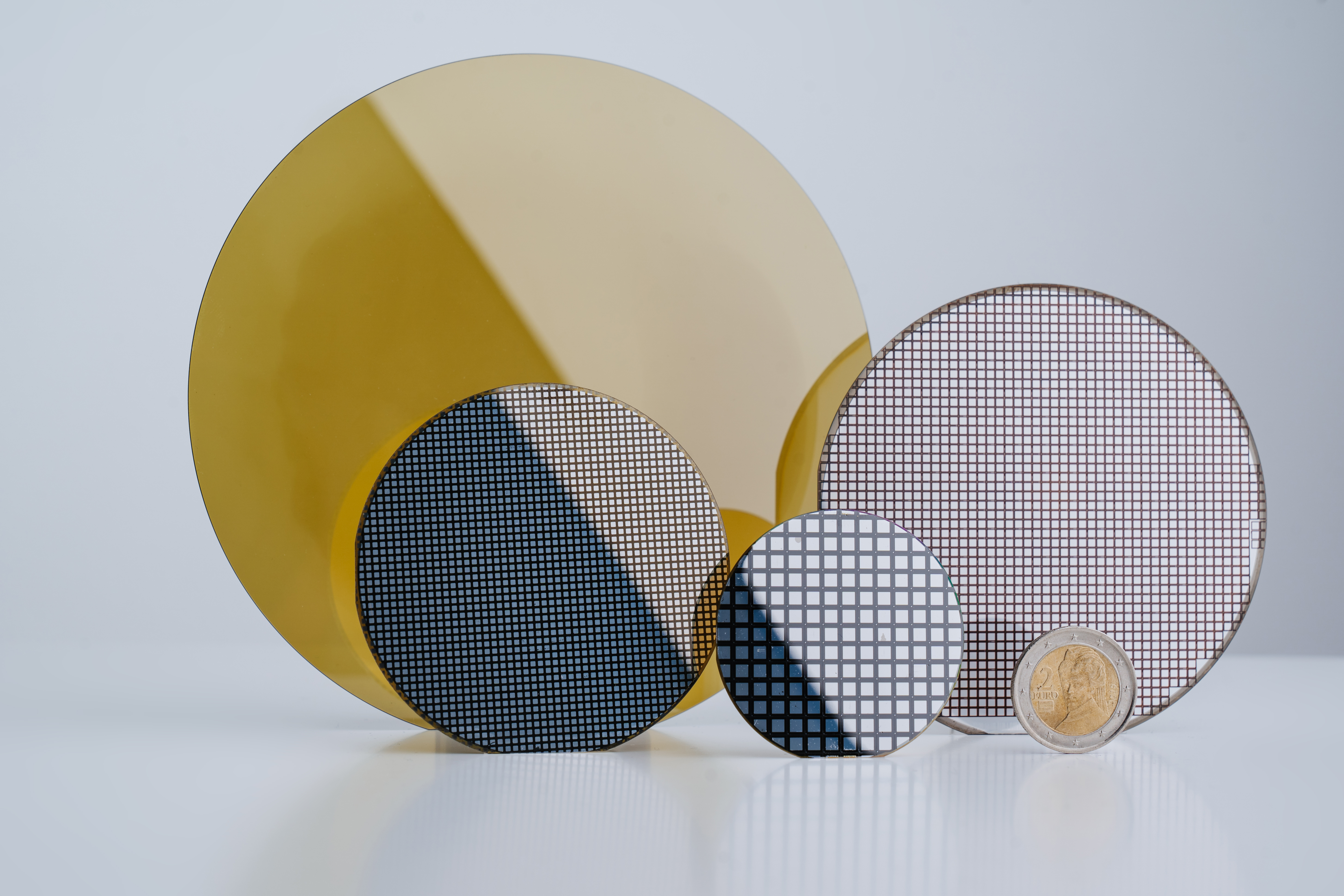
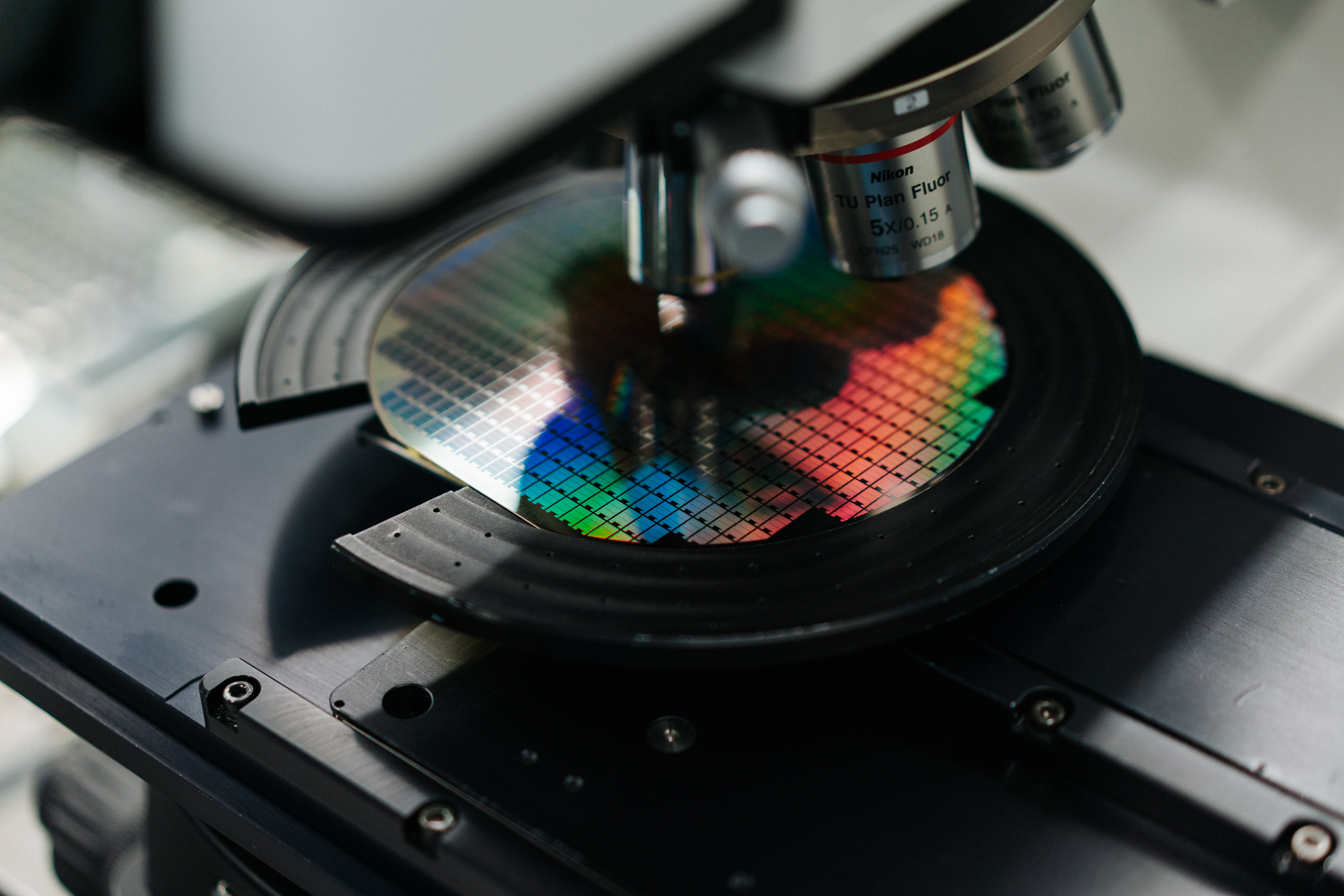
And while silicon wafers in Villach's clean rooms are up to 300 mm in size, other semiconductor materials are only just beginning to be produced: the first silicon carbide chips were produced on 2-inch (50 mm) wafers as early as 2001. A number of hurdles had to be overcome in the process: Not only did the production team have to learn how to handle the new material, but they also had to process the tiny wafers in a line designed for diameters of 4 and 6 inches.
But the Villach production facility also proved to be an optimal breeding ground for SiC wafers: in 2010, the transfer to 4 inches succeeds, and when the Villach site becomes a global competence center for new semiconductor materials in 2017, our SiC wafers have already grown to 6 inches. The last 4-inch lot leaves the site on 12 December 2017.
Press Photos
-

-
-
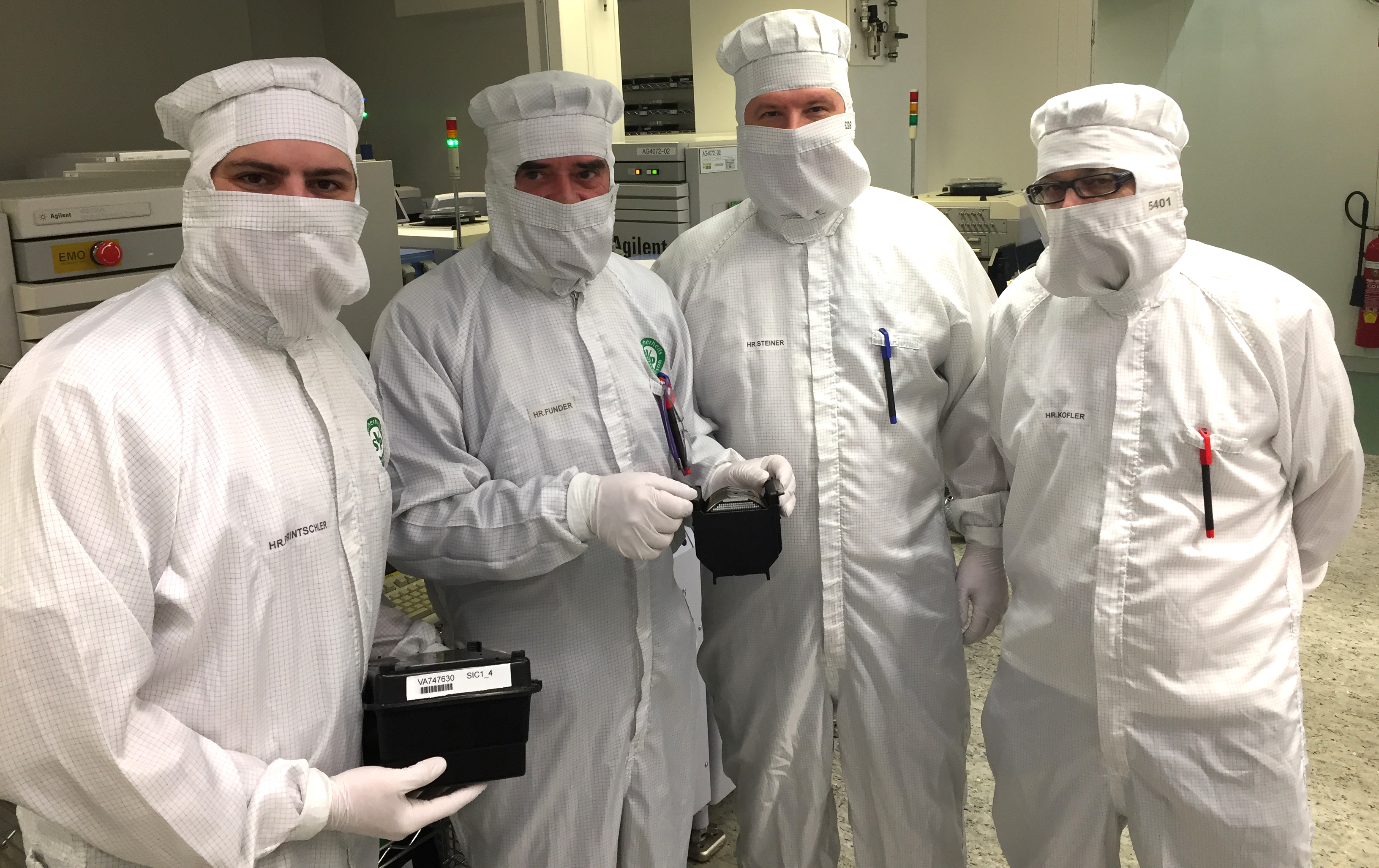
 Martin Printschler, Franz Funder, Bernd Steiner and Josef Koflersic-team
JPG | 3.48 mb | 3264 x 2055 px