SoC & SiP & FPGA
System on Chip (SoC) integrated circuits: Faster and more efficient through higher integration level

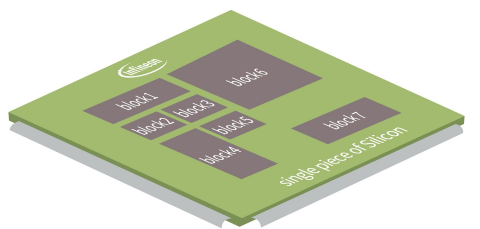
A system on chip (SoC) is an integrated circuit on a single piece of silicon containing all components required to operate a system. System on chip ICs offer many benefits and can offer also embedded microcontrollers, as not only do they consist of multiple operating components, but they are also efficient, compact, and cost-effective to produce. For these reasons, SoCs are continually growing in popularity among system designers and can be found in most systems focusing small form factors or lowest power, like Internet of Things (IoT), smartphones, cameras, embedded systems, and as of the last couple of years, even small PCs and laptops.
A standard system on chip design can include one or more processor cores; a memory system, such as RAM or ROM; external interfaces, such as cable ports (USB, HDMI, etc.) and wireless (WiFi and Bluetooth); a graphics processing unit (GPU), and other components, such as analog/digital converters, voltage regulators and an internal interface bus. Despite their compact size, system on chip ICs are extremely efficient and will often out-perform systems build up with standard components
Application-specific integrated circuits (ASICs) are a type of system on chip IC that is specially designed for use with certain customized applications. This can include both hardware and software.
System in Package (SiP)

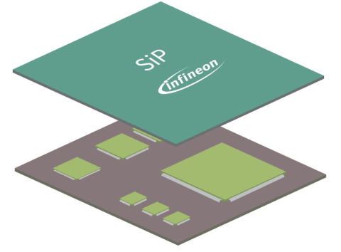
A system in package will be used when functionality should be integrated which requires multiple ASIC technologies, e.g. a high voltage start up cell implemented in a high voltage technology which supports 1200V operations together with some e.g. state-machines, sensors or ADCs implemented in a standard CMOS technology. Infineon as one of the leading ASIC suppliers in the world supports system in packages from simple wirebonded chip-by-chip solutions down to substrate based micro modules with even embedding of dies and several layers.
Field programmable gate array (FPGA)

A field programmable gate array (FPGA) is an integrated circuit that can be reprogrammed multiple times after it has been manufactured. Unlike ASICs, FPGAs can be modified numerous times, which is why they are commonly used by engineers to either do prototyping or to build up system solutions which will be manufactured in lower volumes. Field programmable gate arrays are important for circuit designers, as their reprogrammable features allow for the repair of errors, saving time and money in the short-term. They also allow for multiple iterations of a circuit and can be used to generate fast adaptions in systems during the design process to verify functionality of the entire system or to allow early generation of firmware and software. Afterwards the FPGA will be used for production or the proven functionality will be then used to build up an ASIC.
The primary differences between a FPGA and an ASIC are programmability and cost. A FPGA is ‘field programmable’ meaning it can be modified and reprogrammed without the need to return it to the manufacturer, but are quite costly reaching up to 3 digit $ ranges. Because of the extremely high cost, they cannot be used when the system solution is produced in higher volumes.
ASICs, on the other hand, are integrated circuits designed for specific customized applications that once created, cannot be modified. A full custom IC or ASIC can be easily 10x to 30x cheaper and is the right choice for high(er) volume products. You only have to invest one time for the more complex development, but can enjoy the lower cost for the entire lifetime of your product. To avoid costly and timely iterations during an ASIC development, we use FPGAs in many of our ASIC projects for early prototyping and debug of the entire or partial functionality of the future ASIC.
Once the prototype is built and fully tested for design errors, the ASIC including additional features e.g. analog.


