700V CoolMOS™ P7
700 V CoolMOS™ P7 n-channel superjunction MOSFETs - our answer for flyback topologies
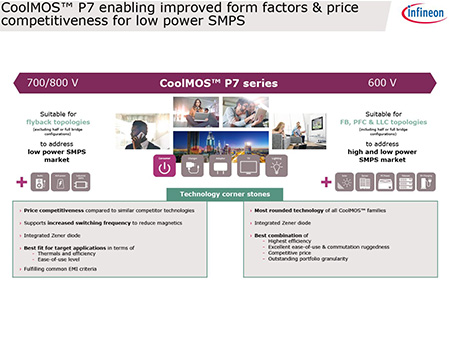
The 700 V CoolMOS™ P7 n-channel superjunction (SJ) MOSFET series has been developed to serve today’s and, especially, tomorrow’s trends in flyback topologies. The technology addresses the low power SMPS market, mainly focusing on mobile phone chargers and notebook adapters, but suitable for power supplies, used within lighting applications, home entertainment (TV, game consoles or audio), as well as auxiliary power supplies.
700 V CoolMOS™ P7 SJ MOSFET family achieves outstanding efficiency gains of up to 4% and a decrease in device temperature of up to 16°C compared to competition. In contrast with the previous 650 V CoolMOS™ C6 technology, it offers 2.4% gain in efficiency and 12°C lower device temperature, measured at a flyback based charger application, operated at 140kHz switching speed.
Benefit from the 700 V CoolMOS™ P7 n-channel superjunction MOSFET family's cost-competitive technology. The products feature low swtiching losses, great thermal behavior and allow high-speed switching.

Keeping the ease-of-use in mind, Infineon kept an eye on launching the technology with a low VGS(th) of 3 V and a very narrow tolerance of ±0.5 V. This makes the P7 easy to design-in and enables the usage of lower gate source voltage, which makes it easy to drive and leads to less idle losses.
To increase the ESD ruggedness up to HBM class 2 level, 700 V CoolMOS™ P7 has an integrated Zener diode. This helps to support increased assembly yield, leads to less production related failures and, finally, manufacturing cost savings on customer side.
Key features
- Highly performant technology
- Low switching losses (Eoss)
- Highly efficient
- Excellent thermal behavior
- Allowing high-speed switching
- Integrated protection Zener diode
- Optimized VGS(th) of 3 V with very narrow tolerance of ±0.5 V
- Finely graduated portfolio
Key benefits
- Cost-competitive technology
- Further efficiency gain at higher switching speed
- Supporting less magnetic size with lower BOM costs
- High ESD ruggedness up to HBM class 2 level
- Easy to drive and design-in
- Enabler for smaller form factors and high power density designs
- Excellent choice in selecting the best fitting product


