AC-DC power conversion for telecom infrastructure
Two-stage power converter | PFC: CCM totem pole (hard switching) | DC-DC: LLC topology (soft switching)
Infineon provides system solutions for powering e.g. 5G small cells and base stations. Applications that require the highest efficiency (99 percent) and high power density (73 W/in3 ), such as high-end servers and telecoms. Converter system designers trust on Infineon Wide Band Gap (WBG) (CoolGaN™ and CoolSiC™) and Super Junction (SJ) (CoolMOS™) power semiconductors combined with Infineon‘s gate driver ICs and microcontroller, combined with Infineon‘s gate driver ICs and microcontroller.
Especially Infineon CoolGaN™ devices are designed to meet typical telecom rectifier applications like industry lifetime and quality (cumulative failure rate) targets when operated in the totem pole, hard switching PFC topology.
With Infineon‘s semiconductor products, you solve the typical AC-DC power converter requirements for use in telecom systems requirement like:
- High efficiency combined with a high power density
- High reliability, in order to minimize maintenance cost
- Low mechanical profile
- Outdoor harsh environmental operation, often in natural convection cooling
- Flat efficiency (typically from 30% to 100% load)
System diagram: Telecom power supply system diagram
Application studies show clear value for e-mode GaN HEMTs in high power designs. GaN HEMTs allow us to push both efficiency and density frontiers.
- Totem-pole Power Factor Corrector (PFC), hard switching configuration e.g. at 65 kHz (e.g. demo board EVAL_2500W_PFC_GAN_A)
- DC-DC section uses an LLC (soft switching) topology (e.g. demo board EVAL_3K6W_LLC_GAN)
- Systems specified for 100% operating time with 15 year lifetime and operate between standby and 80-100% load with a given load profile.
- Typical quality requirement profile targets a cumulative failure rate of 1 FIT at 15 years
Infineon semiconductors are often used for example for a bi-directional capability. Ready to go reference designs like EVAL_3K3W_TP_PFC_SIC board is intended for telecom applications. The totem pole implemented in the EVAL_3K3W_TP_PFC_SIC board operates in Continuous Conduction Mode (CCM) in both rectifier (PFC) and inverter mode, with full digital control implementation on the Infineon XMC™ 1000 series microcontroller.
Find Infineon‘s recommended products for Telecom AC-DC power conversion in the above block diagram, and discover reference designs and available boards to speed up your journey.

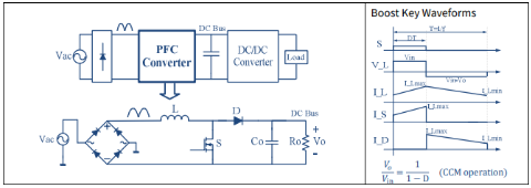
Power Factor Correction (PFC) shapes the input current of the power supply to be in synchronization with the AC input voltage, in order to maximize the real power drawn from the mains (AC supply). In a perfect PFC circuit, the input current is in phase with the input voltage (as it would be with a pure resistor), without any input current harmonics. Although active PFC can be achieved in several ways, the boost converter is the most popular topology used in PFC applications.
For low power applications, the critical conduction mode (CrCM) boost topology has advantages in power saving and improving power density. At some medium/high power level the poor filtering ability and high peak current start to have significant disadvantages.
For high power applications, the continuous conduction mode (CCM) boost topology is the better choice.
Recommended products for your CCM topology are:
- Power controller: PFC continuous conduction mode ICs, Arm® Cortex® 32-bit Microcontroller (MCU) PSoC and XMC
- Gate driver IC: EiceDriver™ gate driver ICs for MOSFETs, IGBTs, SiC MOSFETs and GaN HEMTs
- PFC boost diode: CoolSiC™ Schottky Diodes covering 600 V and 650 V to 1200 V Schottky diodes
- CCM dual boost—MOSFET: CoolMOS™ C7 superjunction MOSFET offers best-in-class performance in PFC. 600V CoolMOS™ P7 superjunction (SJ) MOSFET is the successor of the 600V CoolMOS™ P6 series. It continues to balance the need for high efficiency against the ease-of-use in the design process.
- CCM dual boost—IGBT: TRENCHSTOP™ 5 IGBT technology in a high power package with an extra Kelvin emitter pin. The TO-247 4pin provides ultra-low inductance to the gate-emitter control loop and brings the next level of best in class switching performance.
- CCM totem pole—GaHEMT: GaN-based solutions benefit in-efficiency in the range of 0.3% at significantly reduced complexity. CCM controlled GaN PFC stages with only one HF totem-pole leg is feasible and more cost-effective on system level due to e.g. savings in magnetic components.
Application studies show clear value for e-mode GaN HEMTs in high power designs. It also showed that GaN allows us to use easier control schemes such as CCM modulation in the PFC due to its hard switching capabilities, while at the same time offering performance benefits compared to the next best Si alternative. For Infineon’s CoolGaN™ portfolio of switches and dedicated GaN EiceDRIVER™, are the perfect choice for hard-switching CCM controlled AC-DC power conversion.
Check the full documentation on a 3kW telecom power supply using either GaN or Si-based HV devices for 230 V ACin and 48V DCout, optimized for 50% of the rated power.
Advantages in the PFC stage:
The result shows a clear system benefit for GaN-based solutions with an efficiency benefit in the range of 0.3% at significantly reduced complexity. Especially the PFC stage will run with GaN devices at fixed frequency using CCM modulation with typically relatively high AC ripple to facilitate natural ZVS switching at least partly across the sinusoidally varying input voltage and different load conditions. One of the main differences of the Pareto optimal designs in the commercially interesting range of 30…40W/inch3 between Si and GaN lies in the PFC stage. The TCM modulation of Si leads to high current ripples and RMS-values of the boost inductor currents.
This mandates the interleaving of two HB totem-pole branches to reduce the input current ripple and to facilitate a reduced EMI filter size. In contrast, for the CCM controlled GaN PFC stages, designs with only one HB totem-pole leg are feasible and more cost-effective on system level due to e.g. savings in magnetic components.
Advantages in the LLC stage:
In the LLC stage, the GaN-HEMT based designs require a lower magnetizing current for soft switching and will need shorter delay times. Alternatively, for the same magnetizing current more parallel GaN switches can be employed in the system. Both alternatives allow to reduce the losses in the LLC stage with GaN.
The optimization shows that both silicon-based, as well as GaN-based designs, take benefit from a 2 stage matrix transformer configuration with primary windings being series-connected and secondary windings being paralleled. Furthermore, full-bridge rectification yields better results than center-tapped configurations. Switching frequencies are typically around 100 kHz for Si-based designs versus 150 kHz for GaN-based designs.


