Silicon Carbide MOSFET Discretes
400 V up to 2000 V CoolSiC™ MOSFET discretes ideally suited for hard- and resonant-switching topologies
Infineon CoolSiC™ MOSFETs are built on a state-of-the-art trench semiconductor process optimized to allow for both the lowest losses in the application and the highest reliability in operation. The discrete CoolSiC™ MOSFET portfolio comes in 400 V, 650 V, 750 V, 1200 V, 1700 V and 2000 V voltages classes, with on-resistance ratings from 7 mΩ up to 1000 mΩ.
CoolSiC™ trench technology enables a flexible parameter-set, which is used for implementation of application-specific features in respective product portfolios, e.g.: gate-source voltages, avalanche specification, short-circuit capability, or internal body diode rated for hard commutation.
The 400 V CoolSiC™ MOSFETs were specially developed for use in the AC/DC stage of AI server PSUs and are also ideal for applications such as solar and energy storage systems. Our range of 650 V CoolSiC™ MOSFETs offer optimized switching behaviors at high currents and low capacitances and are designed for a variety of industrial applications including, servers, telecom, motor drives, and more.
The 750 V and 1200 V MOSFET range is available for both industrial and automotive qualified applications, such as on-board charger/PFC, auxiliary inverters, and uninterruptible power supply (UPS). The selection of 1700 V CoolSiC™ MOSFET is offered with flyback typology that can be used in energy storage systems, fast EV charging, power management (SMPS), and solutions for solar energy systems. Lastly, the 2000 V CoolSiC™ MOSFET offers increased power density and voltage margin, designated for high voltage applications such as fast EV charging, and solutions for solar energy systems.

CoolSiC™ MOSFETs in discrete packages are ideally suited for both hard- and resonant-switching topologies like power factor correction (PFC) circuits, bi-directional topologies, and DC-DC converters or DC-AC inverters. An excellent immunity against unwanted parasitic turn-on effects creates a benchmark in low dynamic loss, even at zero volt turn-off voltage in bridge topologies. Our TO- and SMD offering comes also with Kelvin-source pins for optimized switching performance.
We complete the SiC discrete offering with a range of selected driver IC products fulfilling the needs of the ultrafast SiC MOSFET switching feature. Together, CoolSiC™ MOSFETs and EiceDRIVER™ gate driver ICs leverage the advantage of SiC technology: improved efficiency, space, and weight savings, part count reduction, enhanced system reliability.
CoolSiC™ MOSFETs in discrete housings come along with a fast internal freewheeling diode, thus making hard switching without additional diode chips possible. Due to its unipolar character, the MOSFETs show very low, temperature-independent switching and low conduction losses, especially under partial load conditions.
Our unique silicon carbide (SiC) CoolSiC™ MOSFET discrete products from 400 V up to 2000 V are ideally suited for hard- and resonant-switching topologies such as LLC and ZVS, and can be driven like an IGBT or CoolMOS™, using standard drivers. These robust devices offer superior gate oxide reliability enabled by state-of-the-art trench design, best-in-class switching and conduction losses, highest transconductance level (gain), threshold voltage of Vth = 4 V and short-circuit robustness.
SiC MOSFET 650 V and 1200 V Gate Driver ICs
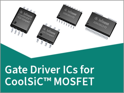
Ultra-fast switching power transistors such as CoolSiC™ MOSFETs can be easier handled by means of isolated gate output sections. Therefore, the galvanically isolated EiceDRIVER™ ICs based on Infineon’s coreless transformer technology are recommended as most suitable.
> More about our EiceDRIVER™ ICs for Silicon Carbide MOSFETs
This video highlights the benefits of CoolSiC™, as seen through the eyes of our customers. Featuring testimonials from alpitronic, Tritium, Lite-On, Siemens Mobility, and Fronius, we see how SiC is driving innovation in energy generation, storage, and consumption.
We are introducing the CoolSiC™ MOSFET with .XT interconnection technology in a 1200 V optimized D2PAK-7 SMD package. SiC MOSFET ohmic conduction losses and fully controllable switching transients are a perfect match with the load profile of such motors. Since the SMD device enables passive cooling for the inverters, they can now be designed maintenance-free.
The presentation will inform you about the specifics of the device. Additionally, the presenting expert will give insights about how maintenance-free inverters can be build up. He will also touch other applications, which are profiting from the CoolSiC™ SMD MOSFET.
Dr. Steffen Metzger explains the technical details of the CoolSiC™ MOSFET in 650V, and highlights the benefits they bring for specific applications. Additionally, he compares the 650 V CoolSiC™ MOSFET with GoolGaN™ and CoolMOS™ and their respective positioning within the greater realm of power semiconductors.
The latest CoolSiC™ MOSFET 650 V is built on a state-of-the-art trench semiconductor process, optimized to allow no compromises in getting both the lowest losses in the application and the highest reliability in operation. It leverages the strong physical characteristics of silicon carbide, adding unique features that increase the device performance, robustness and ease of use.
Thanks to its technological behavior, CoolSiC™ is best-suited for high-power applications. CoolSiC™ sets an industry technology benchmark by combining high performance with robustness and ease-of-use. It enables reliability gains, especially with high temperatures and in harsh environments. Watch this video to learn more about the benefits CoolSiC™ can bring to your designs!
This training will introduce you to the gate oxide reliability of CoolSiC™ MOSFETs and how Infineon's design enables the effective screening of defects by opting for a trench MOSFET.
Additionally, you will understand how this decision has allowed Infineon to achieve high reliability that surpasses that of mature silicon technology without negatively impacting key performance parameters.
Key takeaways
- Be familiar with the target applications for CoolSiC™ MOSFET 750 V
- Know the key features and recognize the benefits
- Understand its positioning compared to other technologies
- Know where to find support material and more information
Discover the benefits and challenges associated with connecting SiC power MOSFETs in parallel
This training talks about the integration of motors and drives with Infineon’s CoolSiC™ MOSFET and how this can help you overcome the limitations of traditional solutions.
This training provides an overview of the 2000 V discrete CoolSiC™ family and explains why it is a right fit for high-power applications.

The switching performance in particular is influenced by the chip's inherent properties, the device's operating conditions and the external circuitry. Optimizing operating conditions and circuitry can significantly improve the device performance in an application.
Circuit designers benefit from SPICE compact models that they can use in computer simulation to understand, troubleshoot and optimize the static and dynamic device behavior of applications through virtual prototyping.
This training explains the characteristics and use cases of simulation models offered by Infineon for CoolSiC™ MOSFETs, what to use them for and how to use them effectively.
- The key features and benefits of the 1200 V CoolSiC™ MOSFET in TO247-4 lead package
- How it addresses the market challenges

Did you know statistics show that the rise in population and economy will drive energy demand to increase by 58% by 2040?
Also, the current climate concerns and geopolitical instability make it even more attractive than ever to generate green, sustainable, and efficient energy, right from home!
Photovoltaic technology, for example, provides a new level of energy independence. Like few other energy sources, solar is accessible directly by consumers and communities, allowing them to build small, independent power grids for personal or collective use.
It is here that Infineon can assist our customers by providing the best-in-class solutions for each application!

As mentioned in the first part, beside social and economic reasons, climate concerns and geopolitical instability make the possibility of generating green, sustainable, and efficient energy right from home very attractive and desirable, and photovoltaic technology provides that level of energy independence.
With that in mind, Infineon is ready to assist our customers, by providing the best-in-class solutions for each application!
Stay tuned, to learn more about it!
By taking this course you will learn more about…
- The gate driving limitation in SiC MOSFETs
- The reason for gate driving limitation parameters in datasheets
- The possible solution to overcome those issues and improve the reliability
Understand why to use WBG switches for bi-directional converters, the topologies used and how they function.
If you want to be an expert of CoolSiC™ discretes and the .XT technology, watch this video!
With the growing market of electrical vehicles, the industry has put forward more requirements for the performance of charging piles.
This e-learning will show you that the emergence of CoolSiC™ MOSFETs has improved the charging pile industry to make the EV charger smaller, faster and with higher efficiency.
This training will introduce you to how the CoolSiC™ will help to design the next generation of servo drives.
Driving a CoolSiC™ MOSFET is much easier than you think. This training will show you how it can be driven with a 0 V turn-off gate voltage.
With this training you will learn how to calculate a reference gate resistance value for your Silicon Carbide MOSFET, how to identify suitable gate driving ICs based on peak current and power dissipation requirements and to fine-tune the gate resistance value in laboratory environment based on worst case conditions.
See how to optimize devices’ behavior in their applications with Infineon’s SPICE Compact Models for CoolSiC™ MOSFETs.
In this video, you will focus on the comparison of the power handling capacity of IGBTs and SiC MOSFETs, Go through the different aspects that need to be considered when dimensioning an IGBT or a MOSFET for a certain application.

- Distinguish the features and benefits of Infineon’s CoolSiC™ solutions in target applications and identify Infineon’s fully scalable CoolSiC™ portfolio to meet this automotive market transition
- Learn about the reasons for the increasing introduction of silicon carbide technology in the automotive applications

By watching this eLearning you will:
- Understand package inductance
- Know why wide bandgap transistors are more susceptible to package inductance, and
- Identify which Infineon package types have lower inductance
Infineon offers trusted expertise in all 3 main power semiconductor technologies. Check out how to position them in AC-DC applications!
Click here to find out more.
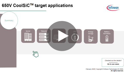
Infineon 650V CoolSiC™ MOSFETs offer a perfect response to the progressing mega trends: more efficiency and power density.
Click here to find out more.

650 V CoolSiC™ technology parameters in a straight comparison with the 600 V CoolMOS™ CFD7.
Click here to find out more.

Get familiar with the main target topologies and the benefits 650 V CoolSiC™ has to offer.
Click here to find out more.

Understand critical design information in order to get the best out of the 650 V CoolSiC™.
Click here to find out more.


