TO-Leadless
Handles currents up to 300 A with substantial footprint reduction
Need a small MOSFET to handle 300 A?
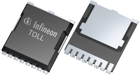
Choose the innovative TO-Leadless package for your high current applications with a 30% footprint reduction whilst eliminating electromigration.
High current applications such as power tools, light electric vehicles and fork lifts often result in MOSFETs being used in parallel, driving up board space and cost - not any longer. Infineon’s TO-Leadless MOSFET package is optimized to handle currents of up to 300 A, increasing power density with a substantial reduction in footprint. A footprint reduction of 30% compared to D²PAK, together with a height reduction of 50%, results in an overall space saving of 60% enabling much more compact designs.
The problem of electromigration is a challenge in high power and high temperature applications as well. Here again TO-Leadless is the ideal package solution. A 50% bigger solder contact area avoids electromigration leading to improvement in reliability. Infineon now offers nine voltage classes for OptiMOS™ power MOSFETs in TO-Leadless ranging from 30 V to 150 V.
Find out more and compare our TOLx products - TOLL, TOLT, and TOLG!
| Key features | Key benefits | Applications |
|
|
|


