sic 碳化硅mosfet-英飞凌(infineon)官网
sic 碳化硅mosfet-英飞凌(infineon)官网 子类别
碳化硅MOSFET解决方案是实现智慧能源世界的重要一步。
英飞凌运用丰富的经验和相关的专业知识,推出了革命性的CoolSiC™ MOSFET技术,这种技术能够实现全新的产品设计。与IGBT和MOSFET等传统的硅基开关相比,碳化硅(SiC)功率MOSFET具有一系列优势。CoolSiC™ MOSFET系列产品覆盖400 V至2000 V的电压范围,适用于光伏逆变器、电池充电、储能、电机驱动、不间断电源(UPS)、辅助电源和开关电源(SMPS)等应用。
碳化硅MOSFET技术
对于系统设计人员而言,碳化硅CoolSiC™ MOSFET技术意味着最佳性能、可靠性和易用性。碳化硅(SiC) 功率晶体管可为设计人员带来新的灵活性,助力实现前所未有的效率和可靠性。高压CoolSiC™ MOSFET技术在反向恢复特性方面也实现了令人印象深刻的诸多改进。
CoolSiC™产品
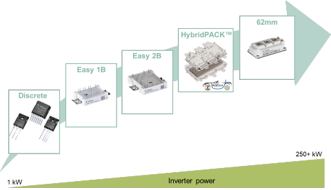
英飞凌的碳化硅CoolSiC™ MOSFET具有高效节能特性和最佳可靠性。该系列产品采用分立封装,还提供650 V、1200 V和1700 V电压等级的模块。CoolSiC™ MOSFET系列包含碳化硅MOSFET分立器件和MOSFET功率模块。其中,SiC MOSFET功率模块拥有三电平、fourpack、半桥、 sixpack和电流扩展等不同配置。
CoolSiC™ MOSFET具备一系列优势。这些优势包括碳化硅开关中的最小栅极电荷和器件电容、反并联二极管无反向恢复损耗、与温度无关的低开关损耗,以及无阈值通态特性等。
英飞凌独特的CoolSiC™ MOSFET可以带来额外的优势。通过最先进的沟槽设计实现出色的栅氧化层可靠性,一流的开关和导通损耗,最高跨导电平(增益),Vth=4V的阈值电压,以及短路稳定性。这是您尽可信赖的革命性器件。
所有这一切带来的是强大的碳化硅MOSFET技术,非常适合硬开关和谐振开关拓扑,如LLC和ZVS,可以像IGBT或MOSFET一样使用易于使用的驱动器进行驱动。由于能在高开关频率下带来最高效率,从而可以减小系统尺寸、增大功率密度,并确保高可靠性,延长使用寿命。
产品阵容
全球首款采用最小和最紧凑封装的高性能1200 V CIPOS™Maxi SiC IPM
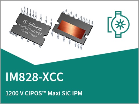
基于CoolSiC™MOSFET的CIPOS™Maxi IPM IM828系列是全球首款1200 V转移模塑碳化硅(SiC)智能功率模块(IPM),它集成了经过优化的6通道1200V SOI栅极驱动器和6个CoolSiC™MOSFET。IM828-XCC是1200 V IPM中封装最小、最紧凑的产品,它将超过4.8 kW的额定功率与出色的功率密度、可靠性与性能结合起来。
> 探索有关CIPOS™ Maxi的更多信息
SiC MOSFET 1200 V门极驱动芯片
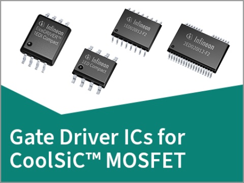
CoolSiC™ MOSFET等超快速开关器件的完美使用需要性能优异的门极驱动。因此,建议选择基于英飞凌无铁芯变压器技术的隔离驱动EiceDRIVER™芯片
This video highlights the benefits of CoolSiC™, as seen through the eyes of our customers. Featuring testimonials from alpitronic, Tritium, Lite-On, Siemens Mobility, and Fronius, we see how SiC is driving innovation in energy generation, storage, and consumption.
This video provides valuable insights into the advantages of WBG (SiC & GaN) technology and its potential impact on the future of renewable energy, especially solar and energy storage systems.
CoolSiC™ MOSFET 网络研讨会
This training will introduce you to the gate oxide reliability of CoolSiC™ MOSFETs and how Infineon's design enables the effective screening of defects by opting for a trench MOSFET.
Additionally, you will understand how this decision has allowed Infineon to achieve high reliability that surpasses that of mature silicon technology without negatively impacting key performance parameters.

The switching performance in particular is influenced by the chip's inherent properties, the device's operating conditions and the external circuitry. Optimizing operating conditions and circuitry can significantly improve the device performance in an application.
Circuit designers benefit from SPICE compact models that they can use in computer simulation to understand, troubleshoot and optimize the static and dynamic device behavior of applications through virtual prototyping.
This training explains the characteristics and use cases of simulation models offered by Infineon for CoolSiC™ MOSFETs, what to use them for and how to use them effectively.
This training provides an insight about the system benefits of wide-bandgap devices, which will conquer market share in areas where power density, efficiency and/or battery range are decisive. The training focuses on two applications, mobile chargers and on-board chargers, and will talk about the challenges faced by the solutions today and how SiC and GaN provide next levels of performance.
观看我们的网络研讨会,了解更多关于硅材料与碳化硅和氮化镓功率器件在高、低功率应用中的技术定位。.
CoolSiC™ MOSFET Microlearnings
This training will introduce you to the gate oxide reliability of CoolSiC™ MOSFETs and how Infineon's design enables the effective screening of defects by opting for a trench MOSFET.
Additionally, you will understand how this decision has allowed Infineon to achieve high reliability that surpasses that of mature silicon technology without negatively impacting key performance parameters.
Key takeaways
- Be familiar with the target applications for CoolSiC™ MOSFET 750 V
- Know the key features and recognize the benefits
- Understand its positioning compared to other technologies
- Know where to find support material and more information
Discover the benefits and challenges associated with connecting SiC power MOSFETs in parallel
By the end of this training, you will be familiar with CoolSiC™ MOSFET 1200 V M1H technology for Easy modules and with Infineon ever-expanding Easy module portfolio in the area of wide band gap material and know about the key features and benefits that are coming along with our latest M1H 1200 V series.
With the growing market of electrical vehicles, the industry has put forward more requirements for the performance of charging piles.
This e-learning will show you that the emergence of CoolSiC™ MOSFETs has improved the charging pile industry to make the EV charger smaller, faster and with higher efficiency.
This training will introduce you to how the CoolSiC™ will help to design the next generation of servo drives.
Driving a CoolSiC™ MOSFET is much easier than you think. This training will show you how it can be driven with a 0 V turn-off gate voltage.
With this training you will learn how to calculate a reference gate resistance value for your Silicon Carbide MOSFET, how to identify suitable gate driving ICs based on peak current and power dissipation requirements and to fine-tune the gate resistance value in laboratory environment based on worst case conditions.
In this video, you will focus on the comparison of the power handling capacity of IGBTs and SiC MOSFETs, Go through the different aspects that need to be considered when dimensioning an IGBT or a MOSFET for a certain application.
- Distinguish the features and benefits of Infineon’s CoolSiC™ solutions in target applications and identify Infineon’s fully scalable CoolSiC™ portfolio to meet this automotive market transition
- Explain the reasons for the increasing introduction of silicon carbide technology in the automotive applications
Infineon offers trusted expertise in all 3 main power semiconductor technologies. Check out how to position them in AC-DC applications!
Click here to find out more.

