Infineon and Giesecke & Devrient Introduce a Leaner, Meaner Chip Card Package; New Production Method Enables to Add Extra Functionality Relatively Quickly and Makes Card`s Chip Package Even Tougher
Joint News Release by Infineon Technologies and Giesecke & Devrient
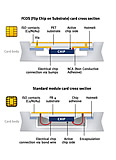
Regensburg, Munich / Germany February 1, 2005 Infineon Technologies AG (FSE/NYSE: IFX) and Giesecke & Devrient GmbH (G&D) have jointly developed an innovative production method for chip packages specifically for use in chip card applications. The FCOS (Flip Chip On Substrate) method unveiled today is the first in which a chip card IC is rotated or flipped inside the module housing it. The functional side of the chip is attached directly to the module by means of conductive contacts; conventional gold wires and synthetic resin encapsulation are no longer required. The new attachment technique saves space in the module; additionally, it is even more robust than the conventional wiring solution. This means that the whole module handles high mechanical stresses better like those encountered, for example, when a chip card is sent by post and passes through the postal systems sorting machines.
Removing the need for the wiring used in existing methods frees up space in the module, which is therefore able to accommodate a larger chip. Typically, the standard maximum chip size has been around 25 square millimetres. Using the new technique, it should be now possible to add extra functionality to the card relatively quickly, without the time- and cost-intensive space optimization work typically required in chip development.
Alternatively, the space savings provided by the FCOS method can be used to shrink the modules in which existing chips are housed. Smaller modules are already in demand for certain applications. The European Telecommunications Standards Institute (ETSI), for example, approved a smaller form factor for SIM (Subscriber Identification Module) cards in mobile phones at the beginning of 2004. ETSI wants to see dimensions of just 12 mm x 15 mm in future, a specification for which the smallest possible modules will be required.
Infineons responsibilities in the FCOS project included the fundamental development work, the design of the module and the development of the production method for FCOS modules. Both companies then brought their expertise to bear to ready the FCOS technology for practical chip card applications. G&D contributed its knowledge of chip card production, built the new module into the card body and conducted all of the card qualification tests necessary to confirm its suitability for high-volume production. Infineon and G&D will each market FCOS independently.
FCOS module technology is ready to go and is suitable for use with the standard production process for smart cards with contacts. The new packaging technology has passed its practical test. Infineon provided the more than 70 million FCOS modules which G&D integrated into prepaid phone cards already in circulation in Mexico.
The FCOS method is in principle suitable for use in all types of chip card including not only prepaid telephone cards and SIM cards for mobile phone network access, but also healthcare cards, personal entitlement cards for access to official services online, bank cards for electronic payment and company ID cards.
The module, the gold contacts which can be seen on the left side of the chip card, is the structure that houses the chip. It connects the chip to the reader and is thus the cards gateway to the outside world. FCOS module technology accommodates memory chips and microcontrollers equally effectively. Conventional chip packages are currently around 580 micrometer (µm) thick on average; FCOS modules not more than 500 µm. A human hair, by way of comparison, is typically around 80 µm thick.
Infineon estimates that it had a market share in excess of 25 percent in 2004 and was thus the worlds leading producer of chip packages for chip card applications. Data from US-based market researchers Gartner shows that Infineon was the world market leader in chips for chip card applications in 2003, supplying approximately 1.1 billion chip card ICs to a market with a total volume of just over two billion units (a market share of 53 percent). Gartner puts the total value of the chip card ICs market in 2003 at around USD 1.26 billion, giving Infineon a market share by sales revenue of 41 percent. According to international growth consultants Frost & Sullivan, G&D is the world's number three manufacturer of chip cards in the year 2003, with a market share of approximately 17 percent of the about two billion chip cards issued in 2003.
Further information about Infineons chip card ICs at: www.infineon.com/security
Further information about smart cards and smart card applications from Giesecke & Devrient available at www.gi-de.com
Giesecke & Devrient (G&D) is a technology leader in the supply of smart cards, systems and solutions for telecommunications, electronic payment transactions, transportation, health, ID, loyalty and multimedia applications as well as Internet security (PKI). G&D is also a leading provider of banknotes and securities as well as currency processing equipment. The Giesecke & Devrient Group, headquartered in Munich / Germany, operates subsidiaries and joint ventures all over the world. G&D employs around 6,800 people world-wide and generates an annual revenue in excess of 1,05 Billion Euro. For more information, visit www.gi-de.com
Regensburg, Munich / Germany February 1, 2005 Infineon Technologies AG (FSE/NYSE: IFX) and Giesecke & Devrient GmbH (G&D) have jointly developed an innovative production method for chip packages specifically for use in chip card applications. The FCOS (Flip Chip On Substrate) method unveiled today is the first in which a chip card IC is rotated or flipped inside the module housing it. The functional side of the chip is attached directly to the module by means of conductive contacts; conventional gold wires and synthetic resin encapsulation are no longer required. The new attachment technique saves space in the module; additionally, it is even more robust than the conventional wiring solution. This means that the whole module handles high mechanical stresses better like those encountered, for example, when a chip card is sent by post and passes through the postal systems sorting machines.
Removing the need for the wiring used in existing methods frees up space in the module, which is therefore able to accommodate a larger chip. Typically, the standard maximum chip size has been around 25 square millimetres. Using the new technique, it should be now possible to add extra functionality to the card relatively quickly, without the time- and cost-intensive space optimization work typically required in chip development.
Alternatively, the space savings provided by the FCOS method can be used to shrink the modules in which existing chips are housed. Smaller modules are already in demand for certain applications. The European Telecommunications Standards Institute (ETSI), for example, approved a smaller form factor for SIM (Subscriber Identification Module) cards in mobile phones at the beginning of 2004. ETSI wants to see dimensions of just 12 mm x 15 mm in future, a specification for which the smallest possible modules will be required.
Infineons responsibilities in the FCOS project included the fundamental development work, the design of the module and the development of the production method for FCOS modules. Both companies then brought their expertise to bear to ready the FCOS technology for practical chip card applications. G&D contributed its knowledge of chip card production, built the new module into the card body and conducted all of the card qualification tests necessary to confirm its suitability for high-volume production. Infineon and G&D will each market FCOS independently.
New FCOS technology already in widespread use
FCOS module technology is ready to go and is suitable for use with the standard production process for smart cards with contacts. The new packaging technology has passed its practical test. Infineon provided the more than 70 million FCOS modules which G&D integrated into prepaid phone cards already in circulation in Mexico.
The FCOS method is in principle suitable for use in all types of chip card including not only prepaid telephone cards and SIM cards for mobile phone network access, but also healthcare cards, personal entitlement cards for access to official services online, bank cards for electronic payment and company ID cards.
FCOS modules: only 6 times thicker than a human hair
The module, the gold contacts which can be seen on the left side of the chip card, is the structure that houses the chip. It connects the chip to the reader and is thus the cards gateway to the outside world. FCOS module technology accommodates memory chips and microcontrollers equally effectively. Conventional chip packages are currently around 580 micrometer (µm) thick on average; FCOS modules not more than 500 µm. A human hair, by way of comparison, is typically around 80 µm thick.
Market position of G&D and Infineon in the smart card sector
Infineon estimates that it had a market share in excess of 25 percent in 2004 and was thus the worlds leading producer of chip packages for chip card applications. Data from US-based market researchers Gartner shows that Infineon was the world market leader in chips for chip card applications in 2003, supplying approximately 1.1 billion chip card ICs to a market with a total volume of just over two billion units (a market share of 53 percent). Gartner puts the total value of the chip card ICs market in 2003 at around USD 1.26 billion, giving Infineon a market share by sales revenue of 41 percent. According to international growth consultants Frost & Sullivan, G&D is the world's number three manufacturer of chip cards in the year 2003, with a market share of approximately 17 percent of the about two billion chip cards issued in 2003.
Further information about Infineons chip card ICs at: www.infineon.com/security
Further information about smart cards and smart card applications from Giesecke & Devrient available at www.gi-de.com
About Giesecke & Devrient
Giesecke & Devrient (G&D) is a technology leader in the supply of smart cards, systems and solutions for telecommunications, electronic payment transactions, transportation, health, ID, loyalty and multimedia applications as well as Internet security (PKI). G&D is also a leading provider of banknotes and securities as well as currency processing equipment. The Giesecke & Devrient Group, headquartered in Munich / Germany, operates subsidiaries and joint ventures all over the world. G&D employs around 6,800 people world-wide and generates an annual revenue in excess of 1,05 Billion Euro. For more information, visit www.gi-de.com
About Infineon
Infineon Technologies AG, Munich, Germany, offers semiconductor and system solutions for automotive, industrial and multi-market sectors, for applications in communication, as well as memory products. With a global presence, Infineon operates in the US from San Jose, CA, in the Asia-Pacific region from Singapore and in Japan from Tokyo. In fiscal year 2004 (ending September), the company achieved sales of Euro 7.19 billion with about 35,600 employees worldwide. Infineon is listed on the DAX index of the Frankfurt Stock Exchange and on the New York Stock Exchange (ticker symbol: IFX). Further information is available at www.infineon.com.
Press contact at G&D
Ulrike Zeitler
Tel.: +49 89 4119 1189, Fax: +49 89 4119 2020, Mobile: +49 160 364 0250
E-mail: ulrike.zeitler@de.gi-de.com
Information Number
INFAIM200502.032
Press Photos
-
 Thomas Tarantino, Head of R&D Module and Embedding Technologies, Giesecke & Devrient GmbHPress Photo
JPG | 572 kb | 1536 x 2048 px
Press PhotoJPG | 5 kb | 120 x 160 px
-
 Christian Juettner, Vice President, Strategic Marketing, Giesecke & Devrient GmbHPress Photo
JPG | 931 kb | 1704 x 2272 px
Press PhotoJPG | 7 kb | 120 x 160 px
-
 Axel Deininger, Senior Director Product Marketing, Security, Automotive, Industrial & Multi-Market business group Infineon Technologies AGPress Photo
JPG | 1.08 mb | 1535 x 2126 px
Press PhotoJPG | 9 kb | 116 x 160 px
-
 Peter Stampka, Marketing Director, Packaging Center, Automotive, Industrial & Multi-Market business group, Infineon Technologies AGPress Photo
JPG | 274 kb | 1063 x 1535 px
Press PhotoJPG | 6 kb | 111 x 160 px
-
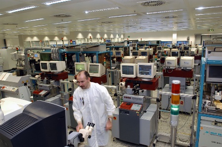 Full house at the Infineon Packaging Center in Regensburg-Burgweinting, GermanyPress Photo
JPG | 864 kb | 3008 x 2000 px
Press PhotoJPG | 8 kb | 160 x 106 px
-
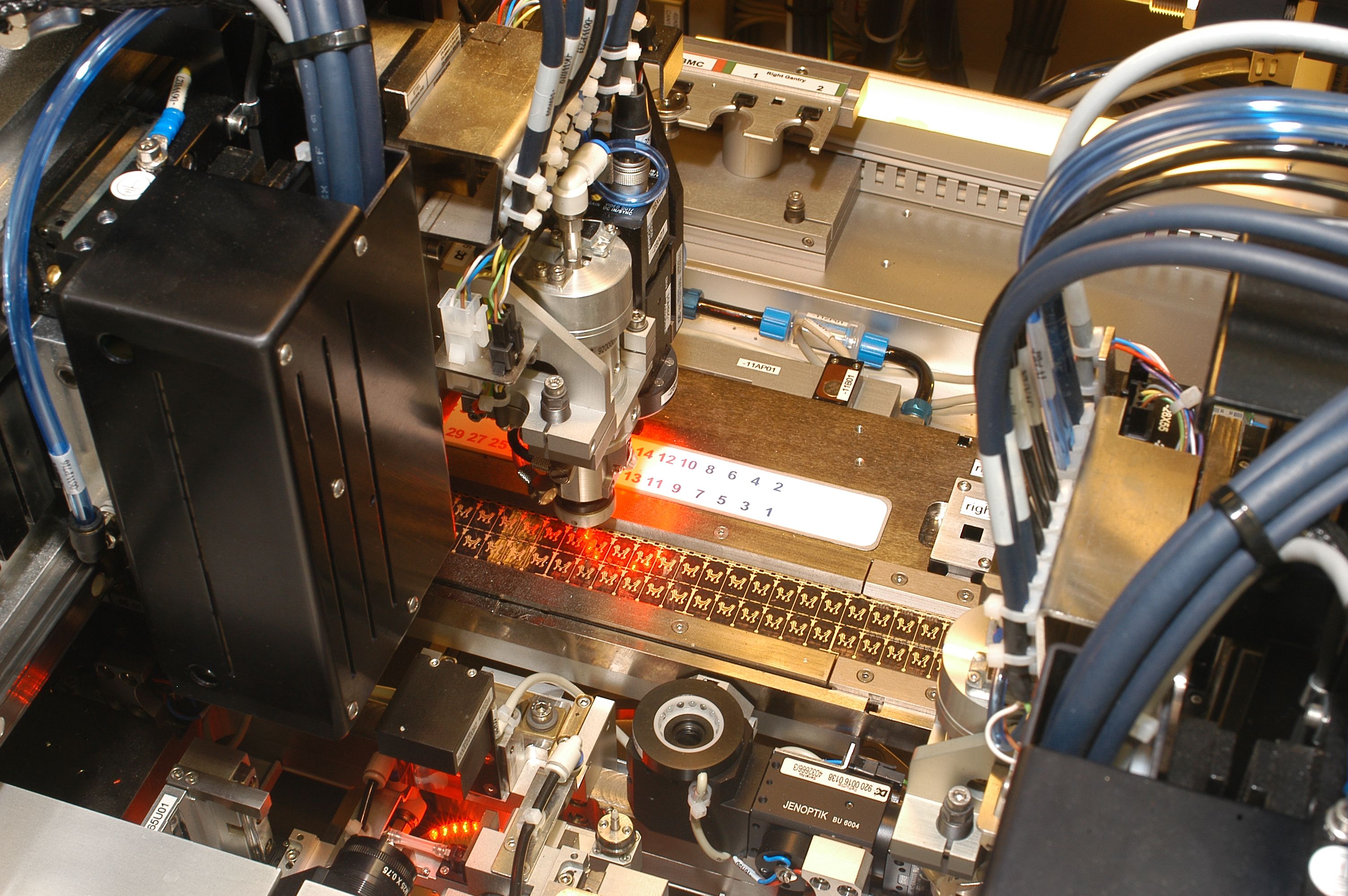
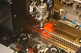
 Detail shot inside the FCOS module line: Two high-precision flip-chip and pick-and-place tools operate simultaneously to attach the chip to the tape, thus creating a FCOS chip card module in less than a second.Press Photo
JPG | 802 kb | 3008 x 2000 px
Press PhotoJPG | 9 kb | 160 x 106 px
-
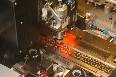 Detail shot inside the FCOS module line: Two high-precision flip-chip and pick-and-place tools operate simultaneously to attach the chip to the tape, thus creating a FCOS chip card module in less than a second.Press Photo
JPG | 744 kb | 3008 x 2000 px
Press PhotoJPG | 7 kb | 160 x 106 px
-
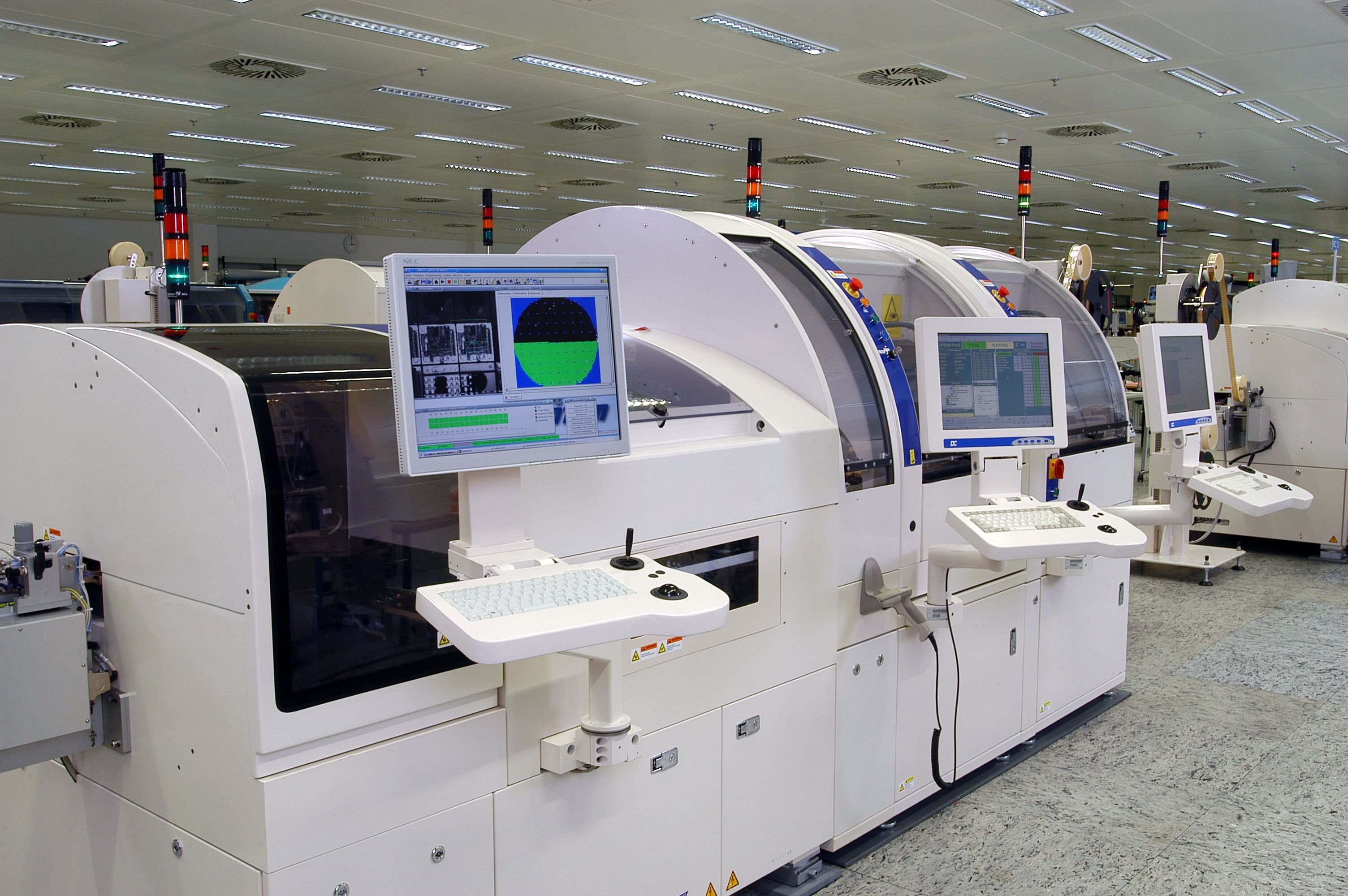
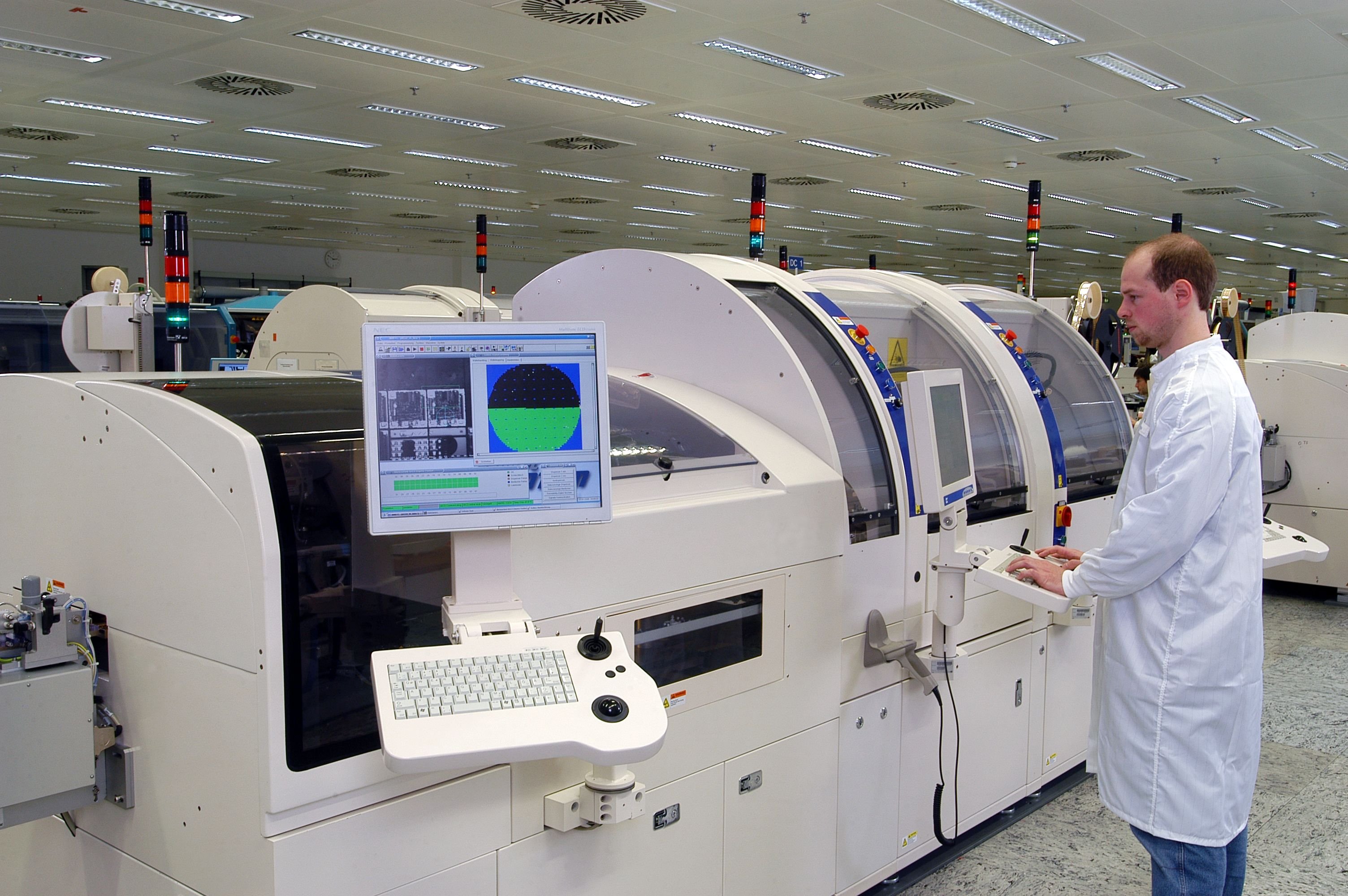
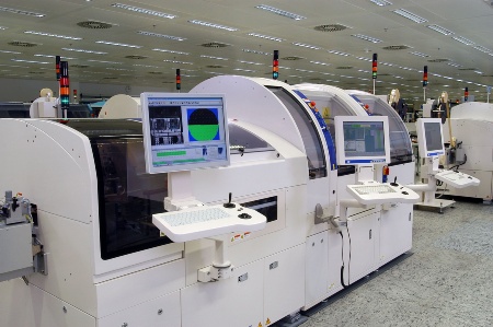 The FCOS (Flip Chip On Substrate) module line at Infineon's Packaging Center in Regensburg-Burgweinting, Germany. FCOS technology is a reel-to-reel fully automated process from bare chip to finished module with inline electrical testing.Press Photo
JPG | 835 kb | 3008 x 2000 px
Press PhotoJPG | 6 kb | 160 x 106 px
-
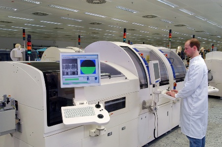 The FCOS (Flip Chip On Substrate) module line at Infineon's Packaging Center in Regensburg-Burgweinting, Germany. FCOS technology is a reel-to-reel fully automated process from bare chip to finished module with inline electrical testing.Press Photo
JPG | 809 kb | 3008 x 2000 px
Press PhotoJPG | 6 kb | 160 x 106 px
-
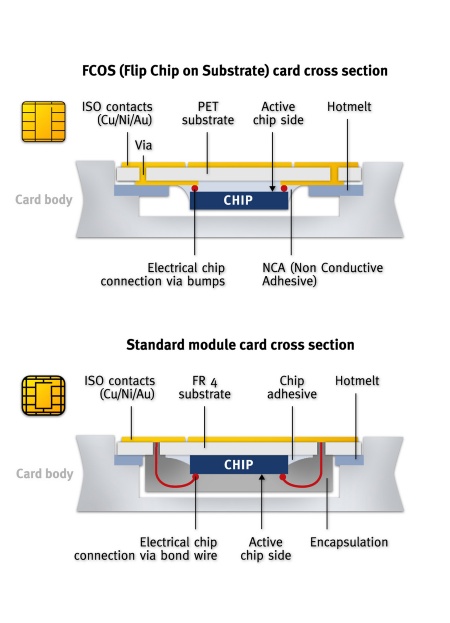 Cross section of a FCOS (Flip Chip on Substrate) module compared to a standard module.Press Photo
JPG | 274 kb | 1535 x 2126 px
Press PhotoJPG | 7 kb | 116 x 160 px