Infineon Technologies Demonstrates Technique To Shrink Wiring of Integrated Circuits To Widths of 40 - 50 Nanometers; Meeting Requirements For Chip Manufacture Into Next Decade
Munich/Germany, May 14, 2001 - Infineon Technologies (FSE/NYSE: IFX) today announced that its Munich Corporate Research Labs have demonstrated that present techniques for integrated circuit wiring can be used for future chip generations, extending to the 2011-2014 timeframe.
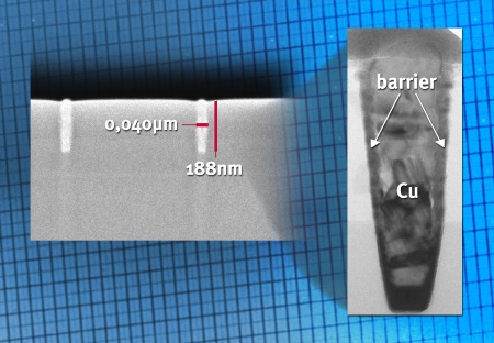
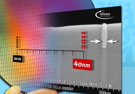
Infineon researchers have successfully produced metal lines, at a width of 40 to 50nm, embedded in the grooves of a dielectric film used for electrical isolation. Such narrow metal lines are used for the shortest electrical connections between the transistors in the chip.
In an electrical assessment of these wires, sufficiently low electrical resistance was verified for all relevant wire lengths. This effectively demonstrates that neither the fabrication of such ultra-thin lines nor the electrical resistance will be technical obstacles for the ongoing process of chip shrinking.
Lithography tools needed for the fabrication of future chip generations in the 2011-2014 timeframe do not yet exist. Infineon overcame this issue by using a spacer technique to narrow the mask openings for pattern transfer into the dielectric film. This allows the production of structures with lateral dimensions far below the feature sizes that can be realized with todays most advanced lithography manufacturing equipment.
This achievement also demonstrates the extendibility of the damascene technique, the state-of-the-art approach in the semiconductor industry to realize advanced chip metallization. In this technique, grooves and holes are filled by depositing metal over the wafer followed by a complete removal of all metal covering the filled structures by chemical mechanical polishing. The technique is named after the way ornaments were once applied in damascene swords.
The silicon wafers used for the demonstration were processed with todays standard semiconductor manufacturing equipment and processes developed for 250nm feature sizes in the cleanroom of International Sematech, Austin, TX, a consortium of the worlds leading semiconductor manufacturers.
The results from Infineons Corporate Research demonstrate that todays wiring technology can be used through the end of the International Technology Roadmap for Semiconductors (ITRS), which extends to 2014. The ITRS describes the technological and material demands of future chip generations.
About Infineon
Infineon Technologies AG, Munich, Germany, offers semiconductor and system solutions for applications in the wired and wireless communications markets, for security systems and smartcards, for the automotive and industrial sectors, as well as memory products. With a global presence, Infineon operates in the US from San Jose, CA, in the Asia-Pacific region from Singapore and in Japan from Tokyo. In the fiscal year 2000 (ending September), the company achieved sales of Euro 7.28 billion with about 29,000 employees worldwide. Infineon is listed on the DAX index of the Frankfurt Stock Exchange and on the New York Stock Exchange (ticker symbol: IFX). Further information is available at www.infineon.com.
Information Number
INFCPR200105.072e
Press Photos
-
 Infineon Technologies Demonstrates Technique To Shrink Wiring of Integrated Circuits To Widths of 40 - 50 Nanometers; Meeting Requirements For Chip Manufacture Into Next DecadePress Picture
JPG | 335 kb | 1535 x 1063 px
-
 Infineon Technologies Demonstrates Technique To Shrink Wiring of Integrated Circuits To Widths of 40 - 50 Nanometers; Meeting Requirements For Chip Manufacture Into Next DecadePress Picture
JPG | 428 kb | 1535 x 1063 px