Infineon Starts to Use 0.11-Micron Process for Volume Production - Worldwide Smallest 256-Megabit DRAM Leads Towards 30 Percent Cost Advantage
Munich/Germany April 29, 2003 Infineon Technologies AG (FSE/NYSE: IFX) today announced that it is using its advanced 0.11-micron process technology for volume manufacturing for DRAMs. Samples of high-density 256Mbit DRAMs manufactured in the new 0.11-micron process have already been successfully validated at Intel and also delivered to strategic partners. The new process results in significantly smaller structures, thus allowing a reduction in the chip size and a production cost advantage per chip of around 30 percent compared to the current volume process technology used by Infineon. The smaller structures compared to the companys previous 0.14-micron DRAM process, allow Infineon to manufacture greater than 50 percent more chips per wafer.
With our new 0.11-micron process, Infineon once again underscores its technology leadership, said Dr. Andreas von Zitzewitz, Member of the Managing Board and Chief Operating Officer of Infineon Technologies AG. Our latest shrink version of the 256Mbit DRAM is the smallest 256Mbit device in the industry. This results from the combination of the ultra-dense 0.11-micron process and our proprietary trench cell technology - which produces approximately 10 percent smaller chip sizes than competitive technologies at same feature size.
The new process was developed at Infineons Dresden 200mm wafer facility and is now ready to start its ramp-up to volume production of high-density and high-speed memories on 200mm and 300mm process lines. During ramp-up at Dresden the new process technology will also be transferred to the other facilities of Infineon`s fab cluster, including Richmond, Virginia, the production joint venture with Nanya called Inotera Memories, and the companys DRAM foundry partner fabs.
Infineon is the first DRAM manufacturer to use the advanced 193nm (nanometer) lithography in volume production for its new 0.11-micron DRAM technology. Future process generations with smaller feature sizes are planned to use the same lithography and will benefit from the experiences already gained. The first products manufactured on the new 0.11-micron technology are 256Mbit DDR components, which are used in personal computers and servers. The transition to smaller process geometries is ideal for production of high-speed memories like DDR2 and Graphics RAM. In addition the smaller feature sizes enable memory densities up to 1Gbit per chip. All DRAM components produced on the process will be based on environmental-friendly technology using lead-free and halogen-free materials.
Combined with Infineons recent announcement that its production of DRAM chips on 300mm wafers had reached cost crossover compared to 200mm wafers, the company continues to reinforce its position as a productivity and cost leader in DRAM manufacturing.
As the pioneers of 300mm technology we have set a new worldwide standard for high-volume semiconductor products. Now we are beginning to reap the production efficiency benefits of our longterm investment in this new technology, said Dr. von Zitzewitz.
Just one year after the start of volume production of memory chips on 300mm-diameter silicon wafers, Infineon produces memory chips since December 2002 at a lower cost per component on 300mm wafers than on 200mm wafers. This crossover allows the company to garner the full benefits of 300mm wafer production; increased productivity and cost savings up to 30 percent for equivalent volumes of memory chips as the plant ramps to full capacity production.
More information about the Infineon range of DRAM products is available at http://www.infineon.com/memory
About Infineon
Infineon Technologies AG, Munich, Germany, offers semiconductor and system solutions for the automotive and industrial sectors, for applications in the wired communications markets, secure mobile solutions as well as memory products. With a global presence, Infineon operates in the US from San Jose, CA, in the Asia-Pacific region from Singapore and in Japan from Tokyo. In fiscal year 2002 (ending September), the company achieved sales of Euro 5.21 billion with about 30,400 employees worldwide. Infineon is listed on the DAX index of the Frankfurt Stock Exchange and on the New York Stock Exchange (ticker symbol: IFX). Further information is available at www.infineon.com.
Information Number
INFMP200304.066
Press Photos
-
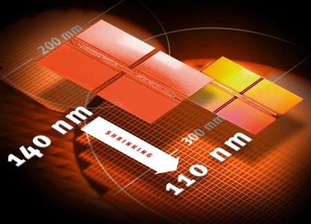 Infineon is using its advanced 0.11-micron process technology for volume manufacturing for DRAMs. Samples of high-density 256Mbit DRAMs manufactured in the new 0.11-micron process have already been successfully validated at Intel and also delivered to strategic partners. The new process results in significantly smaller structures, thus allowing a reduction in the chip size and a production cost advantage per chip of around 30 percent compared to the current volume process technology used by Infineon. The smaller structures compared to the company's previous 0.14-micron DRAM process, allow Infineon to manufacture greater than 50 percent more chips per wafer.Infineon_110nm
JPG | 600 kb | 2126 x 1535 px
Infineon_110nmJPG | 14 kb | 160 x 116 px